Micro-LED Far-Field Emission
A flip-chip InGaN/GaN micro-LED is a light source sitting inside a one-dimensional optical cavity: the quantum well emits between a back aluminium mirror and a top GaN/SiO₂/air exit. That cavity reshapes the far-field electroluminescence (EL) into a wavelength-dependent angular pattern — directional at some wavelengths, ring-shaped at others. This case rebuilds the paper's 1D emitting-dipole model in Dreapex TMM and checks whether the Emission solver reproduces three reported results: the angle-versus-wavelength radiance map (Figure 3b), the per-wavelength directivity of three dies with different GaN thicknesses (Figure 4d, Figure 5c, Figure 5d), and the light-extraction efficiency (LEE) of the same cavity.
The objective is not a point-by-point curve overlay. It is to test whether a strict 1D dipole-in-microcavity model reproduces the shape of the emission pattern (which wavelengths are forward-directed, which form off-axis lobes), the die-to-die shift of that pattern with GaN thickness, and the magnitude of the LEE.
Background
Emission from a horizontal dipole placed inside a planar stack is governed by the classical dipole-in-microcavity (Chance–Prock–Silbey) formalism: the layered environment modifies both the total power the dipole radiates (the Purcell effect) and how that power is distributed over emission angle. For a high-index GaN cavity closed by a metal mirror, most of the emission is trapped as waveguided and evanescent modes; only the fraction inside the air escape cone reaches the far field, and interference in the cavity concentrates that fraction into lobes whose angle depends on the ratio of cavity thickness to wavelength.
The paper is a strong benchmark for a 1D solver because it reduces a real device to a fully specified planar stack: a single horizontal-dipole plane at a fixed depth in GaN, a back aluminium mirror, and a top SiO₂/air exit. Every parameter needed to rebuild it — layer thicknesses, mirror material, emission wavelengths — is given, and the reported directivity varies strongly and non-trivially with wavelength, so a match is meaningful rather than automatic.
Paper Details
- Paper: Study of Far-Field Electroluminescence Emission to Enhance Micro-LED Performance
- Authors: F. Rol, S. Altazin, N. Michit, B. Miralles, C. Ballot, B. Aventurier, P. De Martino, P. Le Maitre, J. Simon
- Journal: Journal of the Society for Information Display 33, 1123-1134 (2025)
- DOI: 10.1002/jsid.2114
- Comparison targets:
Figure 3b,Figure 4d,Figure 5c,Figure 5d
The reproducible content is the set of 1D optical-cavity simulations. The device's simplified stack (paper Figure 3a) is, from the far-field side inward:
SiO₂—200 nmn-GaN + nid-GaN(variable) — the distance from the quantum well to the GaN/SiO₂ interface- horizontal emitting dipoles at a single depth
nid-GaN + p-GaN(variable) — the distance from the quantum well to the mirrorAluminiummirror —100 nm
with 25 nm of nid-GaN on each side of the dipole plane. Three dies from different wafer positions fix the thicknesses:
| Die | QW → mirror (p + nid GaN) | QW → SiO₂ (n + nid GaN) |
|---|---|---|
Die 1 (center) | 202 nm | 634 nm |
Die 2 | 207 nm | 654 nm |
Die 3 | 204 nm | 699 nm |
Mapping the Paper to the TMM Model
The reconstruction runs through the real application flow: the model is built in Structure, the emission is configured in Optics, and the result pages are captured from a live solve. No result page is injected.
| Item | Model used here | Reason |
|---|---|---|
| Far-field / incidence medium | Air | The paper's angular emission is measured in air |
| Top layer | SiO₂ 200 nm (Malitson) | Paper Figure 3a |
| Cavity | Two GaN layers around a thin InGaN QW emissive layer | Reproduces a single dipole plane inside a homogeneous GaN cavity |
| Emitter | One horizontal dipole (Parallel orientation), single depth (Delta distribution), internal quantum efficiency 1 | Paper assumes only horizontally aligned dipoles at a single depth, unity IQE |
| Emission spectrum | File spectrum digitized from the measured EL spectrum (paper Figure 4a) | Uses the real InGaN blue EL band peaking near 462 nm instead of a flat spectrum |
| Back mirror | Aluminium 100 nm (McPeak) | Paper Figure 3a |
| GaN index | Isotropic ordinary index n_o(λ) | Horizontal in-plane dipoles emit light polarised orthogonal to the c-axis, so they see the ordinary index; the paper likewise treats GaN with a scalar index |
The quantum well is modelled as a thin (2 nm) emissive InGaN QW layer carrying the dipole, sandwiched between an n-side GaN layer and a p-side GaN layer. Splitting the GaN this way places the dipole at one well-defined interior plane so that the QW-to-mirror and QW-to-SiO₂ distances match the paper exactly, while keeping the optical medium homogeneous GaN on both sides.
Parallel (horizontal) orientation. In-plane dipoles radiate light polarised perpendicular to the growth axis, which is why the relevant GaN index is the ordinary index rather than a birefringent pair.Reproduction Target and Acceptance Criteria
This case uses a semi-quantitative, shape-and-magnitude standard. The reproduction is successful if:
- In the angle-versus-wavelength radiance map, a bright forward-directed band appears near the central wavelength, with the radiance ridge bending to larger angles at both shorter and longer wavelengths.
- For
Die 1, the per-wavelength emission is forward-directed at the central wavelengths and forms off-axis lobes at the band edges. Die 2andDie 3, which differ mainly in n-GaN thickness, show the same physics with the forward-directed wavelengths shifted, confirming that GaN thickness re-tunes the pattern.- The LEE from the
Modedecomposition (top out-coupling into air) lands in the same single-digit-percent range the paper reports, with most of the emitted power identified as waveguided/absorbed rather than out-coupled. - Sweeping the GaN thickness at fixed wavelength shifts the emission-peak angle, with the p-GaN thickness having a stronger effect on directivity than the n-GaN thickness.
- The LEE varies with cavity geometry — peaking near a p-GaN thickness of
230 nmand dominated by p-GaN over n-GaN — and with wavelength, reproducing the paper's LEE trends.
Point-by-point radiance values are not required; the paper itself notes uncertainty in the refractive indices and in the exact GaN thicknesses.
Modeling Path in Dreapex TMM
1. Structure
The stack from the incidence (far-field) side is SiO₂ / GaN n-side / InGaN QW / GaN p-side / Aluminium. The InGaN QW row is marked emissive and carries one emitter; the two GaN rows carry the ordinary-index GaN data. Die 1 uses GaN n-side = 633 nm and GaN p-side = 201 nm, which — with the 2 nm QW centred — puts the well 634 nm from the SiO₂ interface and 202 nm from the mirror.

2. Footer Diagnostics
Before each run, the Footer status must read that parameter validation passed. The emissive layer must stay coherent, and the wavelength window must lie inside the coverage of every material's index data. Only then is an emission solve meaningful.
3. Optics — Emission
The emission is configured with three Emission detectors:
Intensity— the far-field angular distribution, swept over emission angle0-89°; over the six wavelength slices430-480 nmfor the directivity comparison, or finely over400-500 nmfor the radiance map.Mode— the out-coupling decomposition (top out-coupling, waveguided, evanescent, absorbed), which yields the LEE.Power Dissipation— the underlying dipole power spectrum versus in-plane wavevector.

4. Emission Spectrum from the Paper
Rather than a flat emitter spectrum, the dipole carries the device's measured EL spectrum, digitized from the paper's Figure 4a (the black dashed "Spectrum" curve of the 200-µm Die 1 driven near 30 A/cm²). It is a blue InGaN band peaking near 462 nm.
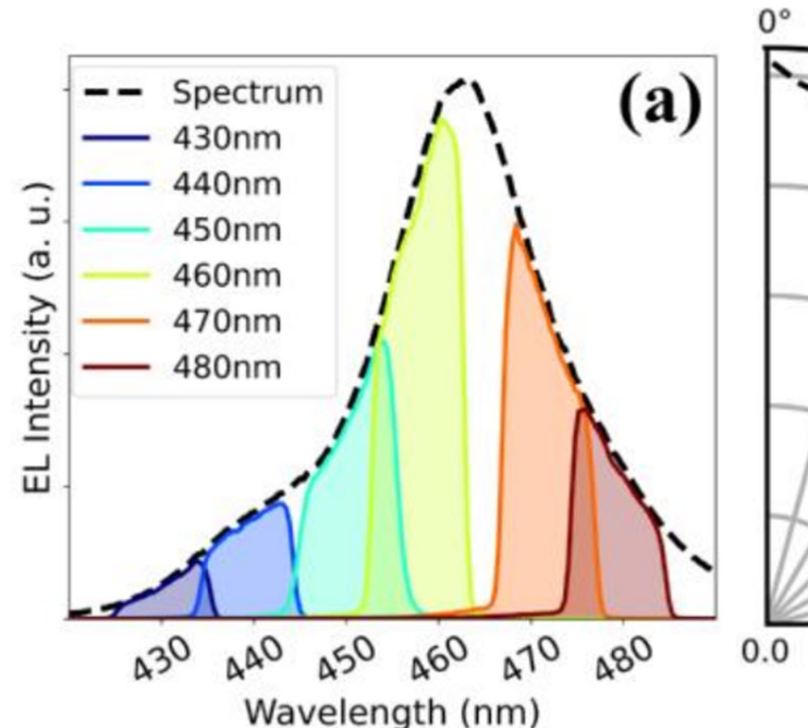
The digitized, peak-normalized spectrum is loaded as a File spectrum on the emitter (Spectrum Type = File):
| λ (nm) | 430 | 440 | 450 | 458 | 462 | 470 | 480 | 488 |
|---|---|---|---|---|---|---|---|---|
| rel. intensity | 0.09 | 0.22 | 0.40 | 0.82 | 1.00 | 0.73 | 0.31 | 0.09 |
For the per-wavelength directivity comparisons, the pattern at each slice is set by the cavity, so the spectrum mainly fixes the relative weight between wavelengths. It becomes essential for the whole-spectrum emission below, where the far field is a spectrum-weighted average over the whole band.
Example Setup
The Die 1 configuration used for the results below:
| Parameter | Value |
|---|---|
| Incidence medium | Air |
| Layer 1 | SiO₂ 200 nm (Malitson) |
| Layer 2 | GaN n-side 633 nm (ordinary index) |
| Layer 3 | InGaN QW 2 nm, emissive |
| Layer 4 | GaN p-side 201 nm (ordinary index) |
| Layer 5 | Aluminium 100 nm (McPeak) |
| Emitter | Parallel orientation, Delta distribution, position 0.5, IQE 1 |
| Emitter spectrum | File, digitized EL spectrum from paper Figure 4a (peak 462 nm) |
| Directivity sampling | wavelength 430-480 nm step 10 nm; angle 0-89° step 1° |
| Map sampling | wavelength 400-500 nm step 4 nm; angle 0-89° step 2° |
Die 2 and Die 3 reuse this configuration with GaN n-side / p-side set to 653 / 206 nm and 698 / 203 nm respectively.
Simulation Results and Comparison
Angle versus wavelength (Figure 3b)
The paper's Figure 3b plots the normalised radiance of Die 1 against emission angle and wavelength. Each wavelength row is normalised to its own maximum.
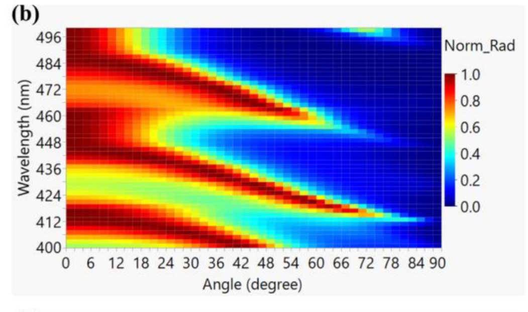
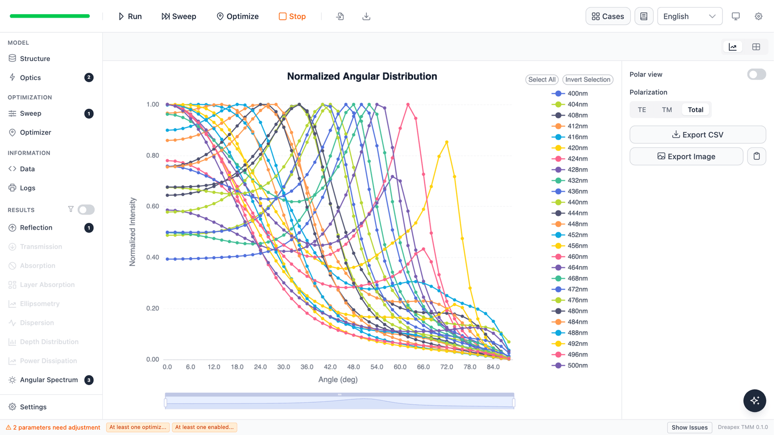
The Dreapex TMM Normalized Angular Distribution over 400-500 nm reproduces the same structure: a forward-directed radiance maximum near 460 nm, with the peak-radiance ridge bending toward larger angles as the wavelength moves away from the central band in either direction. The bright forward band and the diverging high-radiance ridges match the paper's map.
Die 1 directivity (Figure 4d)
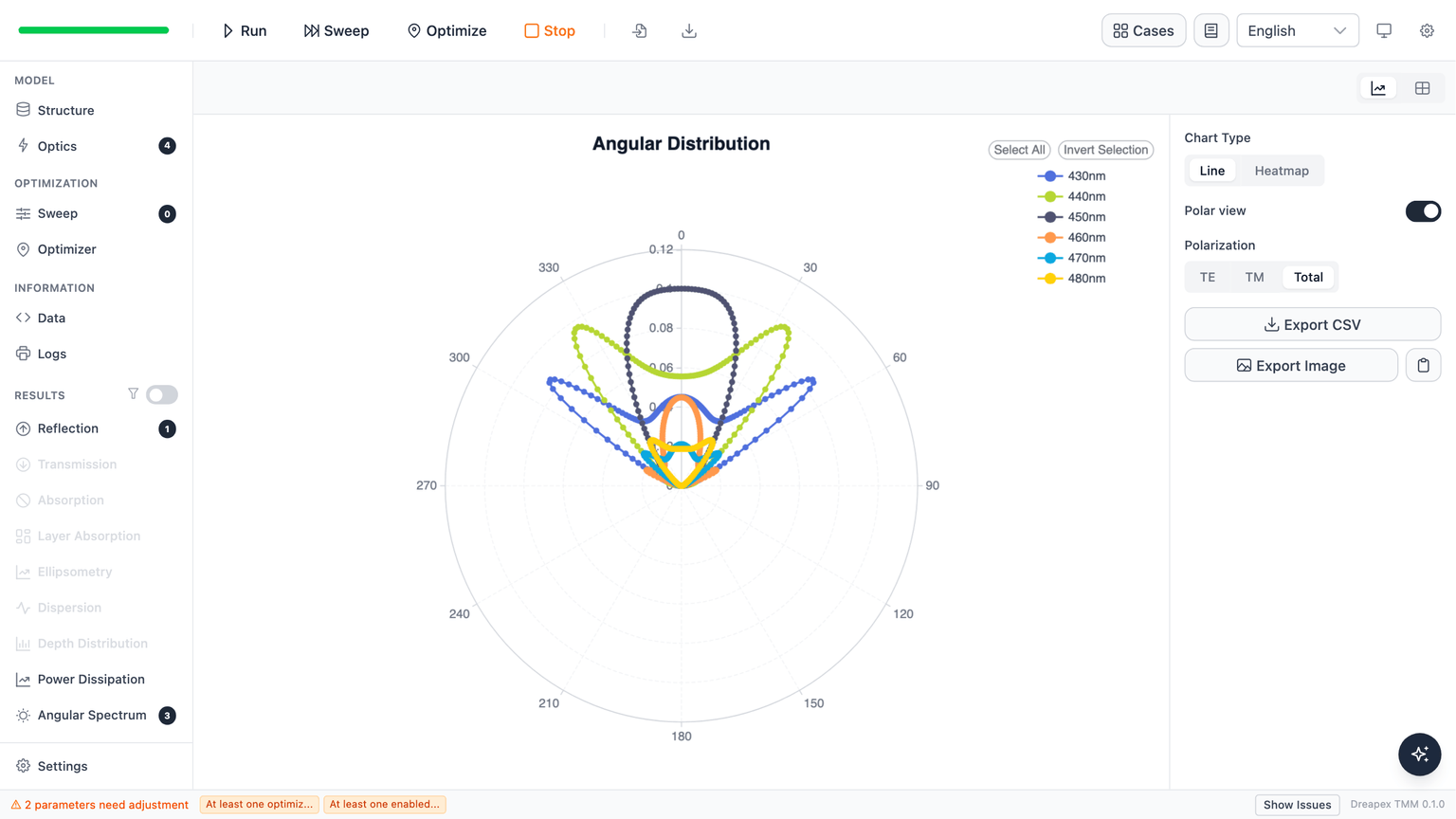
Figure 4 shows the Die 1 emission diagrams per wavelength, experimental on the left and simulation on the right.
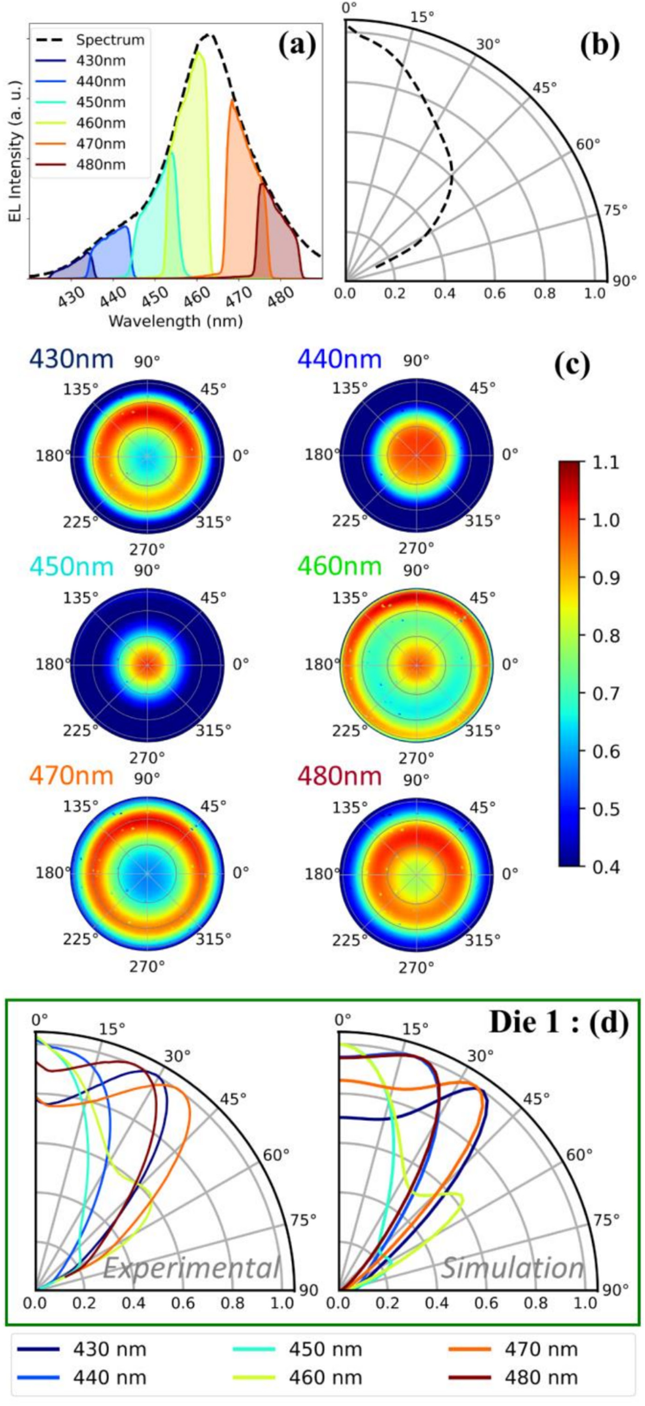
In the Dreapex TMM polar Angular Distribution for Die 1, the six wavelengths split exactly as the paper reports:
| Wavelength | Dreapex TMM pattern | Paper |
|---|---|---|
450 nm, 460 nm | forward-directed lobe at 0° | forward-directed |
440 nm, 480 nm | off-axis lobe near 35° | off-axis lobe |
430 nm, 470 nm | wider off-axis lobe near 50° | off-axis lobe |
Dies 2 and 3 (Figure 5)
Figure 5 compares three dies at different wafer positions. Their p-GaN thicknesses are nearly identical, but the n-GaN thickness grows from 634 nm (Die 1) to 654 nm (Die 2) to 699 nm (Die 3). The paper's central point is that this thickness variation, introduced by wafer thinning, re-tunes the directivity.
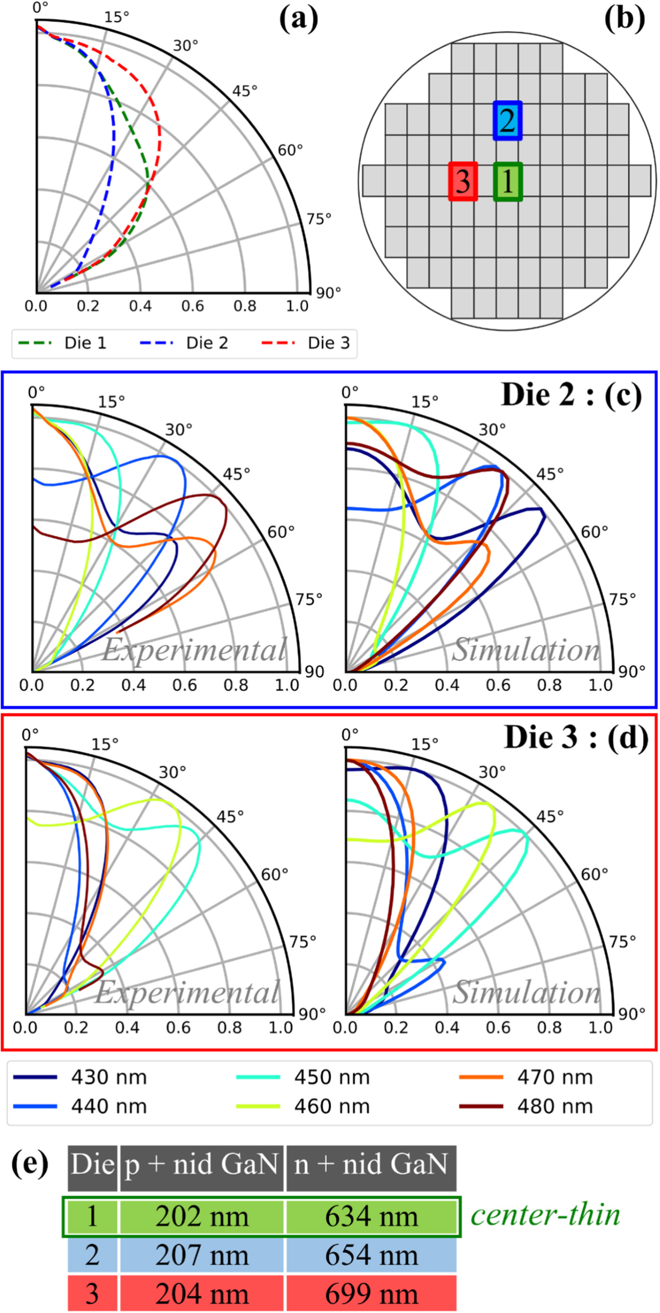
The Dreapex TMM runs reproduce the shift. With the same six wavelengths, the forward-directed wavelengths move die to die: 450/460 nm for Die 1, 430/470 nm for Die 2, 450/480 nm for Die 3. Each die maps wavelength to emission angle differently, exactly because the cavity length has changed.


Directivity versus GaN thickness (Figures 3c and 3d)
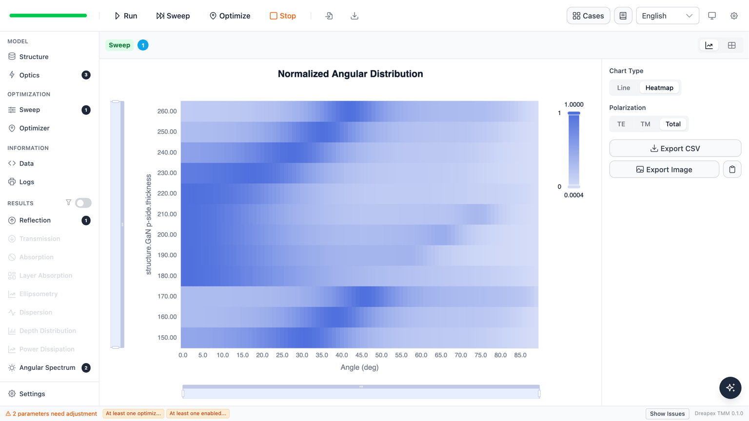
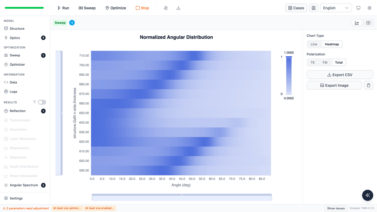
Figures 3c and 3d isolate how the cavity length alone reshapes directivity. Both plot normalised radiance against emission angle and GaN thickness at fixed wavelength — Figure 3c sweeps the n-GaN + nid-GaN thickness, Figure 3d the p-GaN + nid-GaN thickness.
Sweeping the Dreapex TMM GaN p-side thickness from 150 to 260 nm at 460 nm and reading the Normalized Angular Distribution as a heat map reproduces Figure 3d. The emission-peak angle marches outward as the p-GaN thickens: forward-directed at 180-200 nm, splitting into an off-axis lobe near 210 nm, and reaching ~40-45° by 250-260 nm.
The same sweep on the GaN n-side thickness (590-710 nm) reproduces Figure 3c. The peak angle again shifts with thickness, but the forward lobe survives across a wider span and the reshaping is gentler. The p-GaN thickness has the stronger grip on directivity, exactly as the paper reports — the p-side sits between the emitter and the mirror, so it controls more of the cavity round-trip phase.
Whole-spectrum directivity
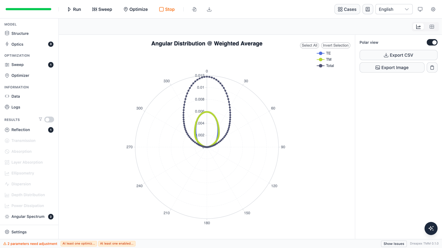
Weighting the emission over the full digitized spectrum (the Intensity detector in Weighted Average mode) gives the far field of the entire EL band in one diagram. The result is a single forward-directed lobe peaking at 0° — the emission is directional, narrower than a Lambertian source. This matches the paper's measured whole-spectrum emission diagram (Figure 2b), where the 200-µm LED is reported as directional relative to cosⁿθ.
Light-extraction efficiency
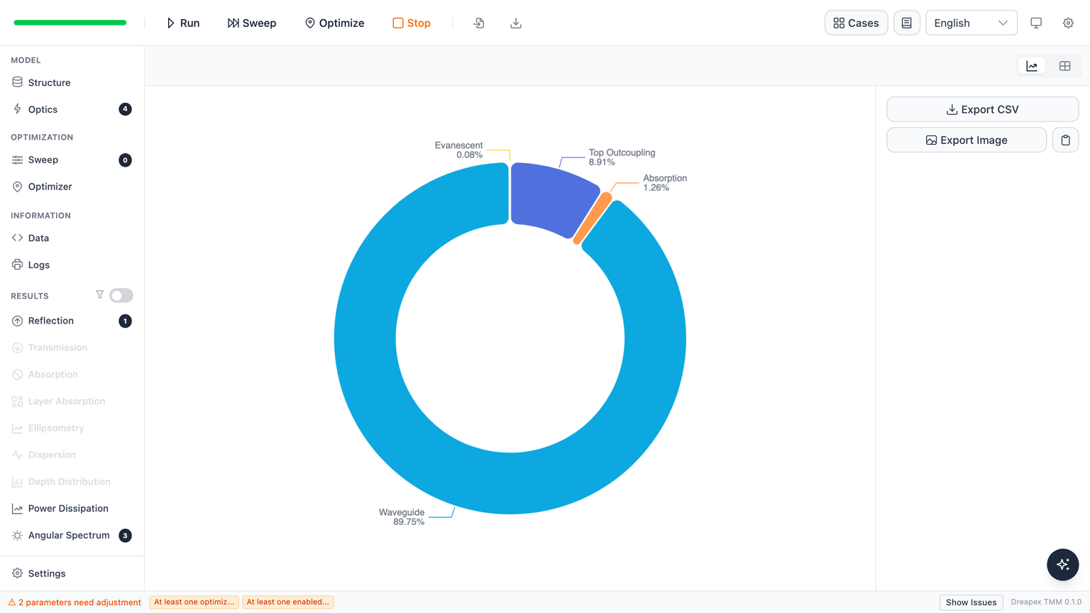
The Mode detector decomposes the dipole's emitted power into out-coupling channels. For Die 1 at 460 nm, the top out-coupling fraction — the LEE into air — is about 9%, with roughly 90% of the power identified as waveguided inside the high-index GaN, a small absorbed fraction in the aluminium, and essentially zero bottom out-coupling (the mirror blocks it). This single-digit-percent LEE, dominated by trapped waveguided power, is consistent with the paper's reported extraction efficiency for these cavities.
LEE versus cavity geometry (Figure 6a)
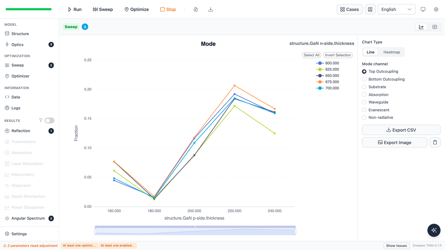
Figure 6a maps the total LEE against both GaN thicknesses, with the nid-GaN fixed at 25 nm. Sweeping GaN p-side (160-240 nm) and GaN n-side (600-700 nm) together and reading the Mode top-out-coupling fraction reproduces it. LEE swings strongly with p-GaN thickness — a minimum near 180 nm and a maximum near 220-230 nm — while the n-GaN thickness (the family of curves) only shifts it slightly. The p-GaN thickness dominates LEE, the same conclusion the paper draws.
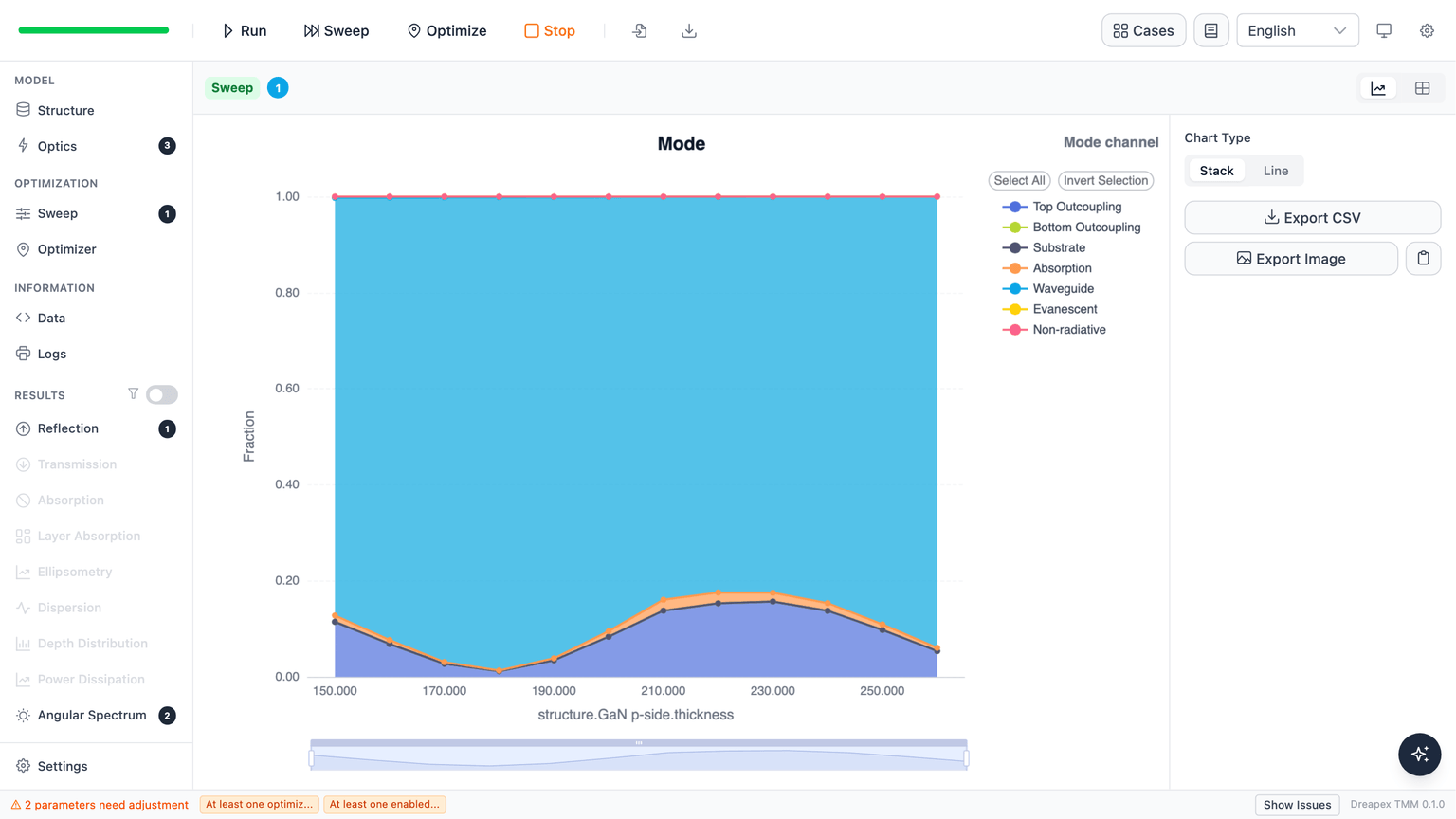
The Die 1 p-GaN of 201 nm sits on the rising flank of that curve. A one-parameter cut makes the design guidance explicit: LEE climbs from about 9% at 201 nm to roughly 16% near 230 nm — nearly doubling for a +25-30 nm change, exactly the improvement the paper predicts for re-tuning the cavity.
LEE versus wavelength (Figure 6b)
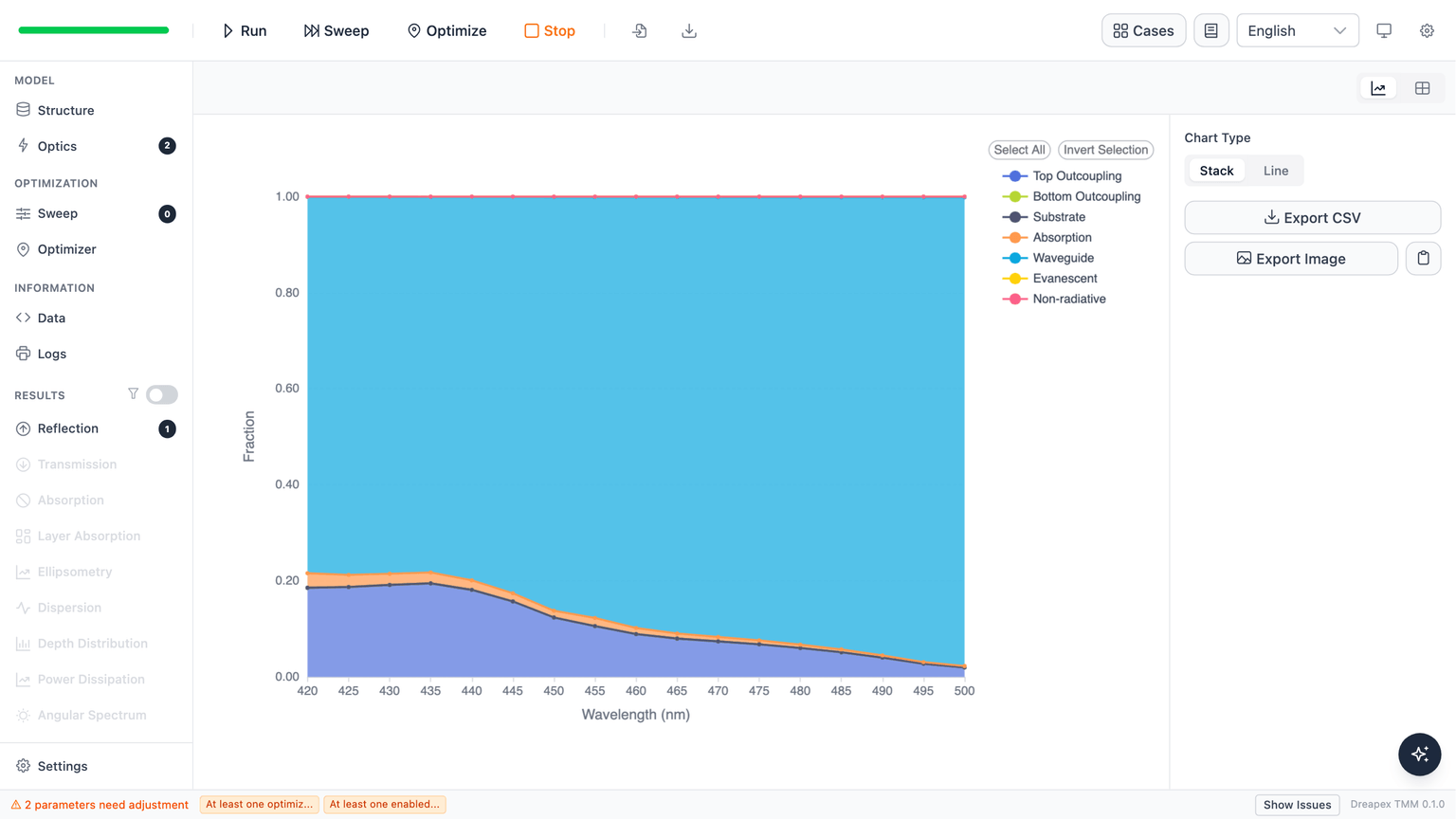
Figure 6b shows the LEE varying with wavelength — a fixed cavity is only optimal over a limited band. Running the Mode detector in wavelength-sweep mode on the fixed Die 1 cavity reproduces the trend: the top-out-coupling fraction is highest near 435 nm (about 20%) and falls steadily to a few percent by 500 nm, passing through ~9% at 460 nm. The cavity extracts efficiently only for the wavelengths it is tuned to.
Deviation Analysis
Several differences from the paper's exact model remain and should be stated explicitly:
- GaN is treated with its isotropic ordinary index. Real wurtzite GaN is weakly uniaxial; that anisotropy is neglected here, consistent with the horizontal-dipole assumption but not identical to a full anisotropic treatment.
- The GaN ordinary-index data is a sparse tabulation across the visible; fine dispersion structure between sample points is linearly interpolated.
- The quantum well is a single
2 nmemissive plane at unity IQE. Injection spread across multiple wells, non-unity IQE, and the exact dipole depth distribution are not modelled. - The aluminium mirror uses one literature dataset; a different metal dataset shifts the mirror phase and therefore the absolute lobe angles.
- The comparison is at the level of pattern shape, die-to-die trend, and LEE magnitude — not a point-by-point radiance fit.
These factors move exact lobe angles and absolute radiance, but they do not change the reproduced conclusions: the wavelength-dependent directivity, its shift with GaN thickness across dies, and the single-digit-percent LEE.
Further Extensions
- Replace the single dipole plane with a depth distribution across the active region to test how injection spread softens the directivity.
- Add a genuine anisotropic (uniaxial) GaN treatment and compare the lobe angles against the isotropic ordinary-index approximation used here.
- Repeat the thickness and LEE sweeps at several emission wavelengths to build the full LEE-versus-geometry-versus-wavelength picture and choose a cavity that balances directivity against extraction.
Ultrathin Absorbing Interference Coatings
Reproduce the calculated reflectivity of thick Au coated with thin Ge films (5/10/15/20/25 nm) from Kats et al. (Nature Materials, 2013), Figure 2c, in Dreapex TMM.
Overview
Validate forward calculations and optimization results against established software, public data, or analytical solutions.