Emission Structure
This guide explains how to model the emissive layers of OLEDs, QLEDs, and PeLEDs as dipole sources inside a film stack. It introduces the model inputs, emission detectors, and main result pages, so you can understand the relationship between the emissive layer, emitters, device structure, and results, and know how to start an emission simulation.
Model Inputs and Result Quantities
Emission uses the layer order, thicknesses, and optical constants already defined in Structure. Its internal source is defined by an EML and one or more Emitters; the incident spectrum, incident angle, and polarization of propagation simulation are not used.
| Physical object | Software setting | Key inputs |
|---|---|---|
| Layered optical environment | Structure | Top and bottom media, layer order, thickness, complex refractive index, coherence |
| Emissive layer | Emis. on the target layer | The EML containing the radiating source |
| Emitter | Emitter inside the EML | Emission spectrum, dipole orientation, position and distribution, intrinsic quantum efficiency, conversion efficiency, lifetime |
| Design variable | Sweep or Optimizer | Electrode thickness, transport-layer thickness, emitter position, and related parameters |
The three emission detectors provide complementary results:
| Detector | Result pages | Main use |
|---|---|---|
Intensity | Intensity, Normalized Spectrum, Normalized Angular Distribution, Intensity Color | Output spectrum, angular distribution, angular color shift, and CIE coordinates |
Mode | Mode, Emission | TOC, BOC, SUB, ABS, WVG, EVA, and NRA fractions, plus Purcell factor, effective quantum efficiency, and lifetime |
Power Dissipation | Power Dissipation | Power versus in-plane wave vector, used to locate propagating light, waveguide peaks, and high-wave-vector SPP/evanescent features |
Mode, see Power Dissipation and Optical Modes: Mode Fractions and Device Efficiency. The case below sets both effective quantum efficiency and conversion efficiency to 100%, so its TOC, LEE, and EQE values are equal.Case: Ag Top Electrode Controls a Top-emitting OLED Microcavity
Load Top-emitting OLED from the Case Library. The preset uses a synthetic Alq3 green spectrum, Isotropic dipole orientation at the center of the EML, an Intensity range of 450–650 nm and 0–80°, and a 530 nm Mode result for this comparison. The stack is shown below.
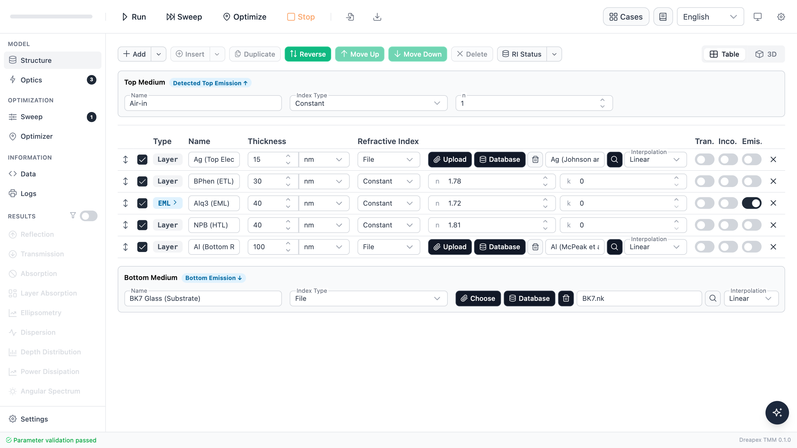
The Al bottom electrode is the high-reflectance mirror. The semitransparent Ag top electrode acts as both the output coupler and the upper mirror. The following real runs change only the Ag thickness to 10 nm and 30 nm; BPhen 30 nm, Alq3 EML 40 nm, NPB 40 nm, and Al 100 nm remain fixed. This isolates the combined effect of top-electrode transmission, reflection phase, and metal absorption.
Output Spectrum
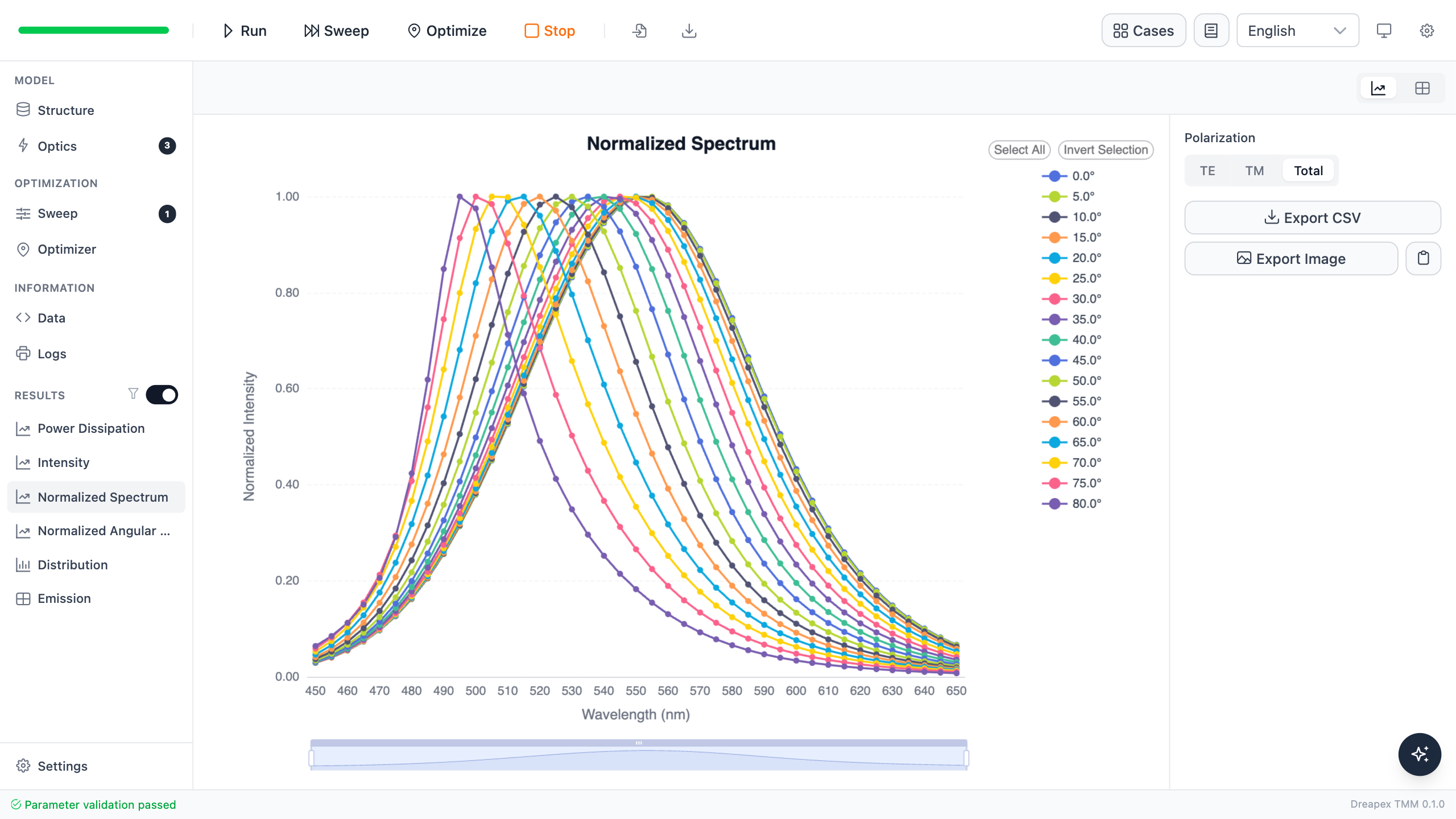
With 10 nm Ag, the normal-emission peak is at 555 nm. Linear interpolation of the half-maximum crossings gives a normal-emission FWHM of approximately 87 nm. The peak shifts to shorter wavelengths as the emission angle increases, producing a broad microcavity spectrum with clear angular dependence.
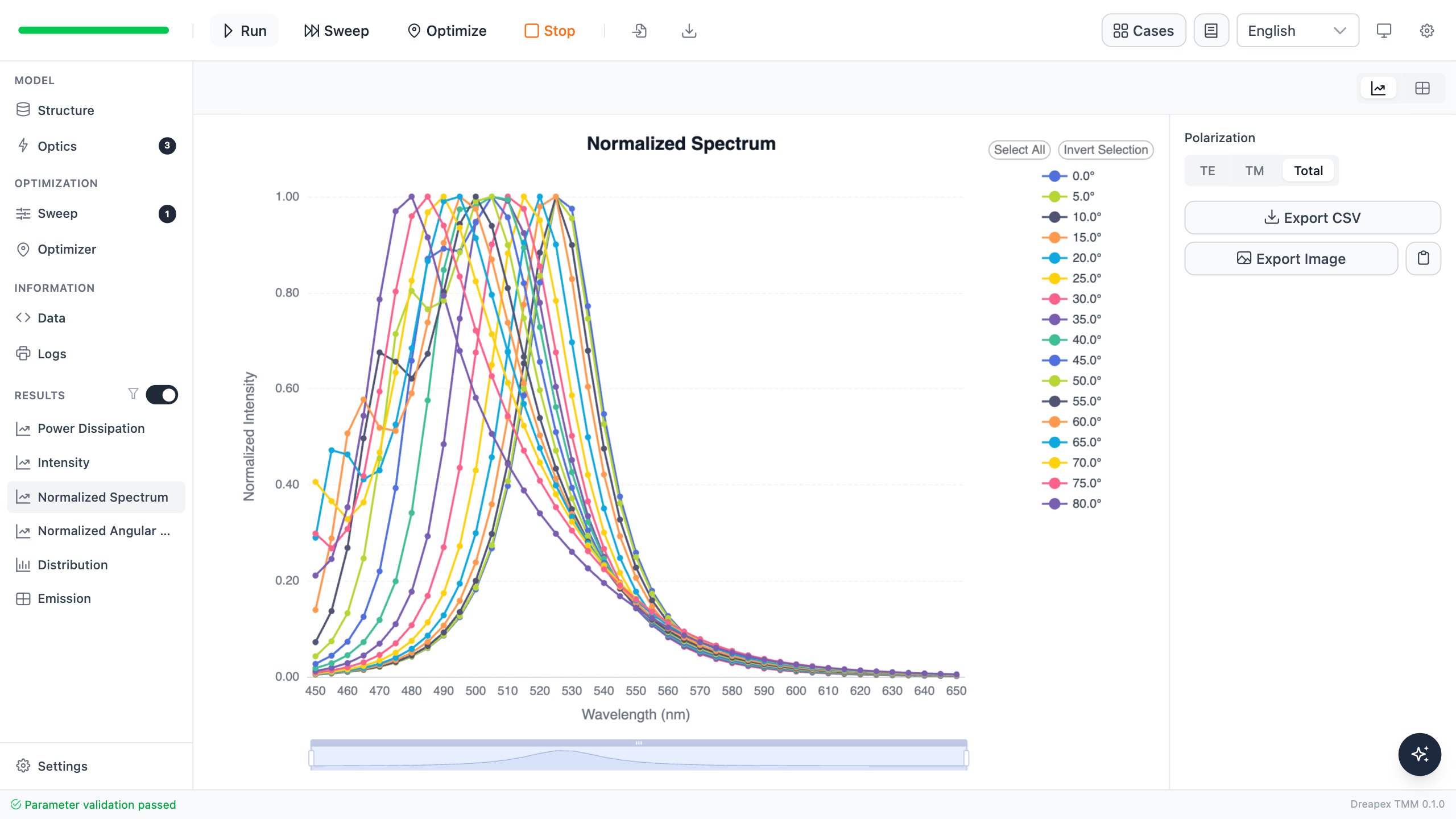
With 30 nm Ag, the normal-emission peak moves to 525 nm and the normal-emission FWHM narrows to approximately 29 nm. The thicker Ag layer strengthens the upper-mirror action and greatly increases the cavity's wavelength selectivity. The peaks at different angles remain clearly separated, so the narrower spectrum is accompanied by stronger angular color shift.
Angular Distribution
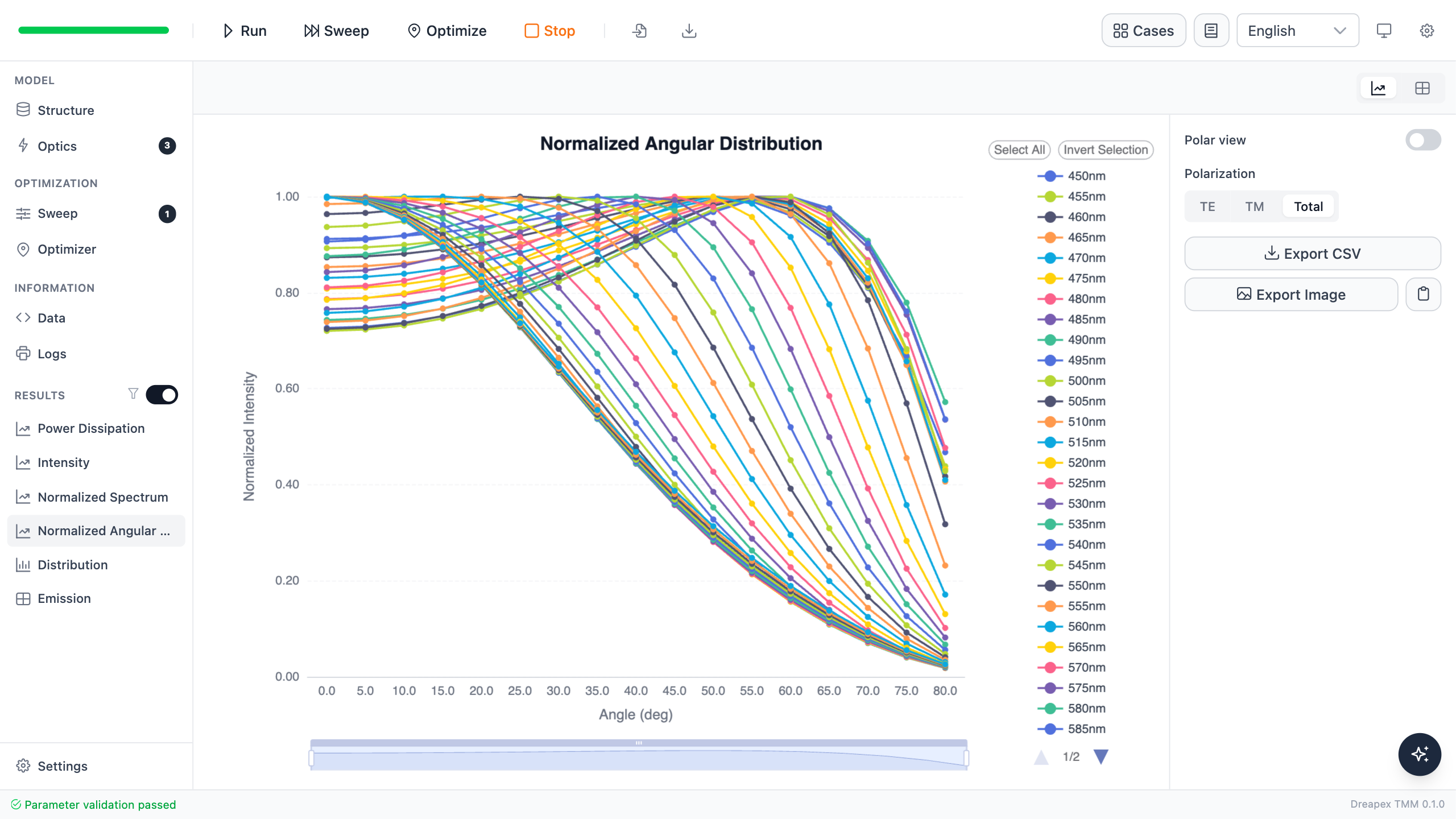
At 530 nm, the 10 nm Ag structure reaches maximum intensity near 40°. After normalization to that maximum, the values at 0°, 30°, 60°, and 80° are approximately 0.84, 0.96, 0.68, and 0.08. The main lobe is broad and displaced from the surface normal.
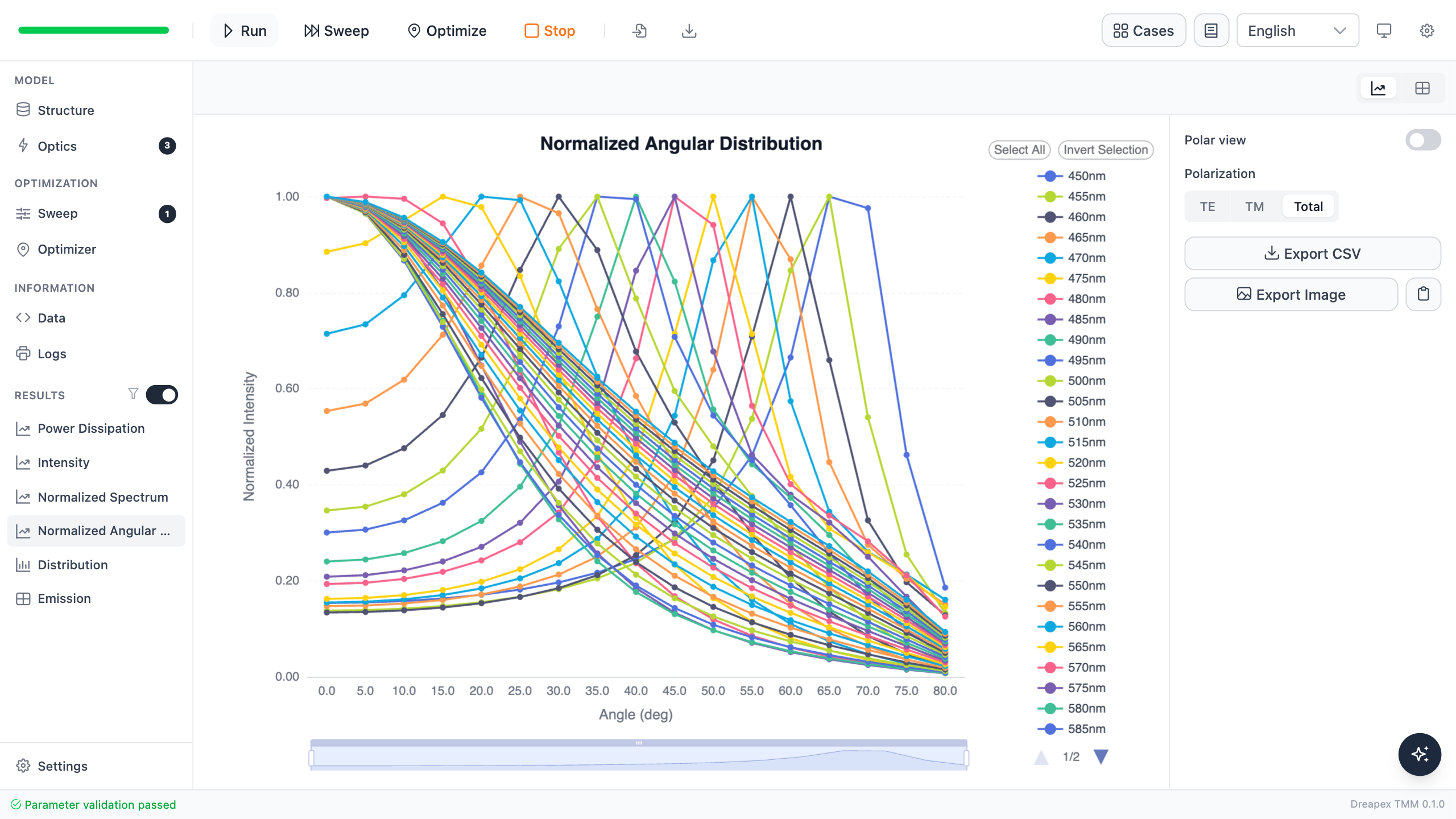
The 30 nm Ag structure moves the 530 nm maximum to 0°. The normalized values at 30°, 60°, and 80° fall to approximately 0.36, 0.05, and 0.007, concentrating the output into a much narrower normal-direction lobe. Together, the spectrum and angular plots show the joint wavelength and propagation-angle selection imposed by the cavity resonance.
LEE, EQE, and Loss Allocation
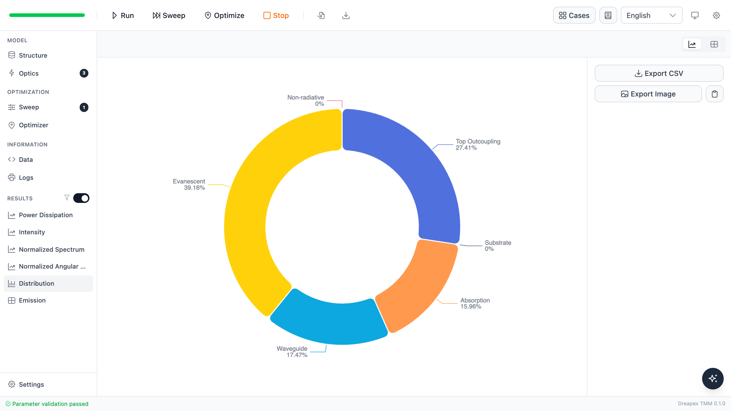
At 530 nm, the 10 nm Ag structure has 27.41% TOC, 15.96% absorption, 17.47% waveguide power, and 39.16% evanescent power. Because the preset sets both effective quantum efficiency and conversion efficiency to 100%, both LEE and EQE are 27.41% in this case.
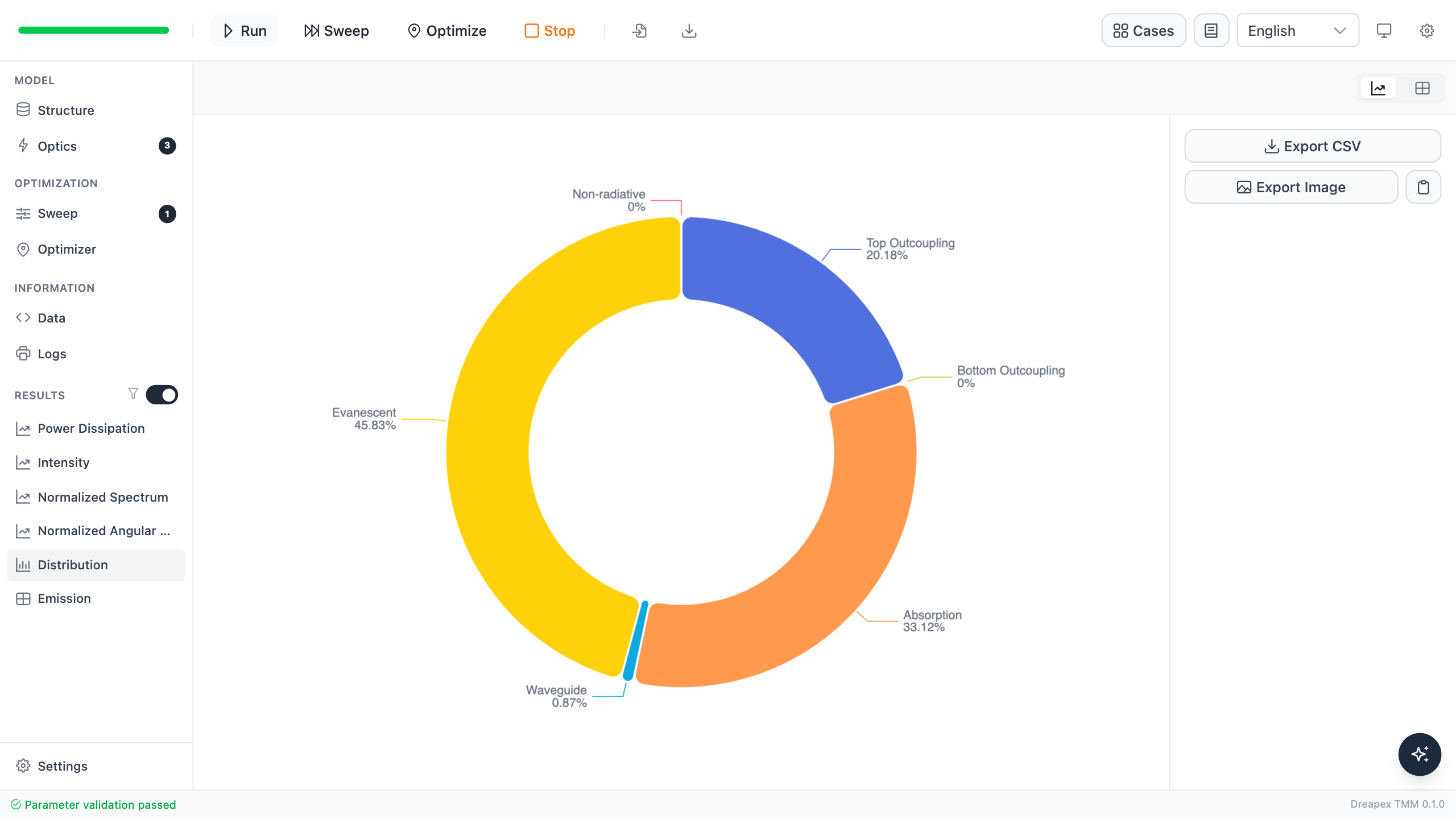
At 30 nm Ag, TOC falls to 20.18%, absorption rises to 33.12%, evanescent power rises to 45.83%, and waveguide power falls to 0.87%. The thicker electrode produces narrower, more normal-directed 530 nm emission but does not improve integrated extraction. Increased metal absorption and evanescent coupling offset the stronger directionality. A taller spectral peak or a narrower main lobe is therefore insufficient as an efficiency metric; it must be checked against the integrated Mode budget.
Further studies can sweep Ag thickness, NPB thickness, or emitter position to isolate the upper mirror, cavity length, and dipole-to-metal distance. See Swept Emission, Emitter Setup, and Emission Detectors for the corresponding settings.
OLED / QLED Optical Analyses
The following papers provide useful examples of connecting structure and dipole sources to spectra, angular results, and mode losses:
| Paper | Device | Analysis to study |
|---|---|---|
| Nowy et al., J. Appl. Phys. 104, 123109 (2008) | OLED | Separates outcoupled, substrate, waveguide, and surface-plasmon losses, then compares emitter quantum efficiency and device geometry |
| Furno et al., Phys. Rev. B 85, 115205 (2012) | OLED | Jointly analyzes Purcell modification, emission rate, modal power, and experiment |
| Salehi et al., Adv. Funct. Mater. 29, 1808803 (2019) | OLED review | Organizes dipole orientation, microcavity effects, internal modes, and extraction structures |
| Zhu, Luo & Wu, Opt. Express 22, A1783 (2014) | QLED | Calculates extraction efficiency, spectrum, angular distribution, and color shift together, including high-index QD-device losses |
| Li et al., Nature Communications 15, 5161 (2024) | Top-emitting QLED | Treats a single-mode microcavity, angle-resolved spectra, angular color shift, and outcoupling in one design |
| Jin et al., npj Flexible Electronics 6, 35 (2022) | QLED | Examines how EQE, angular emission, and measurement conventions affect simulation–experiment comparison |
When reading this literature, check the emitter position and orientation, complex-index data, spectral and angular sampling ranges, mode-integration boundaries, and whether the simulated and measured quantities use the same convention.
Further Modeling
- OLED Outcoupling Efficiency — material quantum yield, device EQE, and the classical extraction limit
- Dipole Model and Applicability — dipole orientation, position distribution, and model boundaries
- Microcavity Effect — spectrum, color, angular distribution, Lambertian behavior, and efficiency
- Power Dissipation and Optical Modes — waveguides, SPPs, and the device power budget
- Purcell Effect — emission rate, effective quantum efficiency, and lifetime
- Emitter Setup — spectrum, orientation, position, distribution, and quantum efficiency
- Emission Detectors — sampling for Intensity, Mode, and Power Dissipation
- Swept Emission — electrode thickness, cavity length, and emitter-position sweeps