OLED Outcoupling Efficiency
An organic emitter may have a quantum yield of 90% while the device EQE remains near 20%. The missing photons are distributed across three stages: charges form emissive excitons, excitons decay radiatively, and the generated light leaves the planar device.
Emission optics primarily addresses the third stage and can also feed back on the second. This article places material metrics, device efficiency, and optical simulation in one loss budget, then uses the classical escape cone to explain the roughly 20% outcoupling scale.
Material Quantum Yield Is Not Device EQE
Photoluminescence quantum yield (PLQY) measures the fraction of absorbed photons that produce emitted photons under optical excitation. OLED external quantum efficiency (EQE) measures how many photons leave the device per injected electron under electrical drive. Exciton formation, nonradiative processes inside the device, and optical trapping still separate these quantities.
Normalizing to one injection event, the device efficiency can be written as
Here, is the external quantum efficiency; is the conversion efficiency from charge pairs to the target emissive excitons, including charge balance and the usable-exciton fraction; is the effective quantum efficiency in the device optical environment; and is the light-extraction or outcoupling efficiency (LEE), the fraction of photons entering electromagnetic emission channels that reaches the target external medium. All three factors are dimensionless and lie between 0 and 1.
Material PLQY is most closely related to the intrinsic emitter quantum efficiency , but it cannot replace , , or . Charge imbalance, exciton quenching, and optical feedback under electroluminescence can all move the device away from the material measurement. Even with , , and ,
This gives the most direct order-of-magnitude explanation for a 90% material yield and a device EQE near 20%.
Classical Escape Cone and Outcoupling Limit
The emissive layer and organic functional layers usually have higher refractive indices than air. When light travels from a high-index to a low-index medium, only directions inside the critical angle can propagate directly across the interface. The critical angle is
where is measured from the interface normal, is the emissive-layer index, and is the external-medium index, with . Plane waves beyond undergo total internal reflection, leaving a finite escape cone.
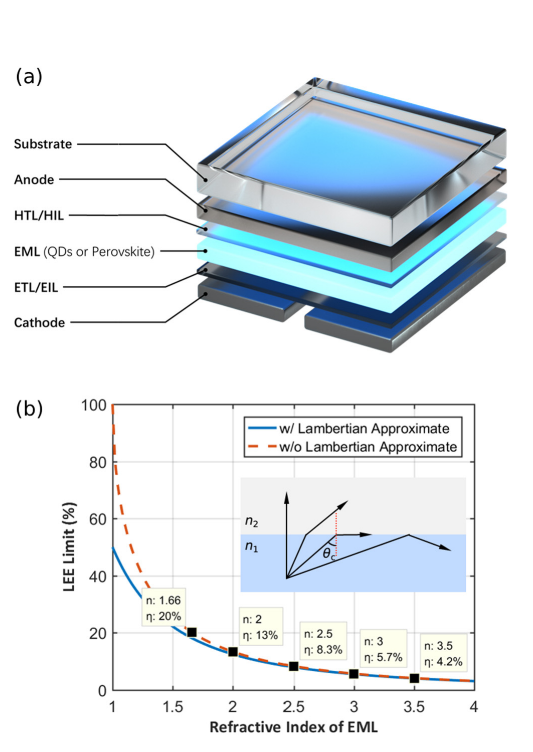
For an isotropic planar emitter with approximately Lambertian emission into air, classical ray optics gives
At , this is about 17%, often summarized as the classical OLED outcoupling scale of roughly 20%. The expression includes only the geometric escape cone and assumes ideal orientation, reflection, and zero absorption. Real OLEDs also exhibit dipole-orientation effects, thin-film interference, metal absorption, waveguiding, and surface-plasmon coupling. The formula is therefore a useful starting intuition, not a final device prediction.
Where the Unextracted Energy Goes
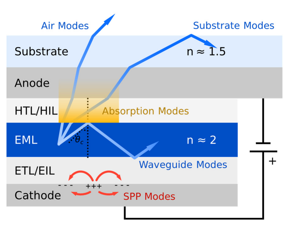
Energy outside the escape cone does not disappear immediately. It enters several channels in the layered structure.
| Energy channel | Origin | Device consequence |
|---|---|---|
| External outcoupling | Wavevector lies inside an external-medium light cone | Produces useful light and contributes to EQE |
| Substrate mode | Light enters a high-index substrate but is totally internally reflected at the substrate–air boundary | Remains trapped in the substrate |
| Waveguide mode | Total internal reflection and interference in organic layers or transparent electrodes | Propagates laterally and is eventually lost |
| Absorption | Metals, electrodes, and lossy functional layers absorb electromagnetic energy | Converts optical energy to heat |
| Evanescent and SPP coupling | Dipole near fields couple to high-wavevector states at a metal–dielectric interface | Often creates strong near-field loss |
| Exciton nonradiative decay | Excitons do not enter an electromagnetic channel | Represented by |
Snell's law alone cannot separate these channels. Film thicknesses are comparable to the wavelength, so reflected waves interfere coherently; the energy allocation must be solved with a dipole multilayer model and integrated in in-plane-wavevector space. See Power Dissipation and Optical Modes for the exact definitions.
Introductory Phenomena and Their Physics
| Observable phenomenon | Main optical cause | Related article |
|---|---|---|
| High material PLQY but device EQE near 20% | Conversion efficiency, effective quantum efficiency, and outcoupling efficiency multiply stage by stage | This article |
| Changing one layer thickness changes brightness and efficiency with the same emitter | Dipole position and microcavity interference redistribute outcoupling and loss | Microcavity Effect |
| A display looks greener, bluer, or more saturated off axis | The cavity resonance moves with angle and reweights spectral bands | Microcavity Effect |
| Some OLEDs are nearly Lambertian while others are strongly forward-directed | A weak cavity can approach constant radiance; a strong cavity selects angles | Microcavity Effect |
| Horizontally oriented molecules often increase EQE | Horizontal dipoles place more power near the surface normal and inside the escape cone | Dipole Model and Applicability |
| Moving the EML toward a metal changes both lifetime and efficiency | The optical environment changes the decay rate and high-wavevector loss | Purcell Effect |
| Increasing electrode reflectance can first raise and then lower efficiency | Constructive interference improves outcoupling while repeated passes and metal absorption grow | Microcavity Effect |
Together, these observations show that the material determines what light can be generated, while device optics determines its color, direction, and probability of leaving the device.
Next Step
Continue with Dipole Model and Applicability to see why an emitter is represented by a point dipole and how molecular orientation enters the calculation.
Reference
- Tsutsui, T.; Takada, N. Progress in Emission Efficiency of Organic Light-Emitting Diodes: Basic Understanding and Its Technical Application. Jpn. J. Appl. Phys. 2013, 52. https://doi.org/10.7567/JJAP.52.110001
- Shim, J. I.; Shin, D. S. Measuring the Internal Quantum Efficiency of Light-Emitting Diodes: Towards Accurate and Reliable Room-Temperature Characterization. Nanophotonics 2018, 7, 1601–1615.
- Greenham, N. C.; Friend, R. H.; Bradley, D. D. C. Angular Dependence of the Emission from a Conjugated Polymer Light-Emitting Diode: Implications for Efficiency Calculations. Adv. Mater. 1994, 6, 491–494.
- Salehi, A.; Chen, Y.; Fu, X.; Peng, C.; So, F. Manipulating Refractive Index in Organic Light-Emitting Diodes. ACS Appl. Mater. Interfaces 2018, 10, 9595–9601.