Dipole Model and Applicability
An OLED emissive layer is not a collection of tiny lamps radiating uniformly in every direction. Each transition dipole has an axis: its far-field radiation vanishes along that axis and is strongest perpendicular to it.
Planar emission simulation represents molecular, quantum-dot, or perovskite emission centers as oscillating electric dipoles, then combines their orientations, positions, and spatial distributions into an emissive layer. This article defines that source model and the conditions under which it represents a real device.
Radiation Pattern of a Point Dipole
When the spatial extent of an emission center is much smaller than the wavelength, its lowest-order radiation can be represented by an electric dipole moment . In free space, the far-field power per unit solid angle obeys
where is the total dipole radiation power, is the power per unit solid angle, is solid angle, and is the angle between the observation direction and the dipole axis. Radiation is zero at and maximal at .
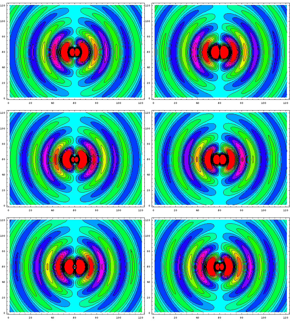
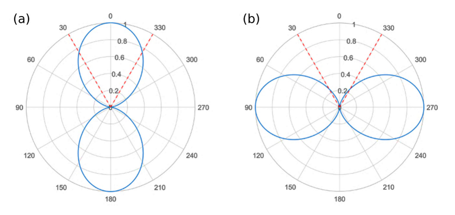
In a planar device, a horizontal or parallel dipole lies in the layer plane, while a vertical or perpendicular dipole points along the layer normal. A horizontal dipole has strong radiation near the normal and couples more readily into the escape cone. For each propagation direction, the wavevector and layer normal define the plane of incidence: the TE electric field is perpendicular to that plane, while the TM electric field lies within it. A vertical dipole has no far-field radiation along the normal and produces only TM components, making coupling to large-angle guided states and surface plasmon polaritons (SPPs)—TM modes bound to metal–dielectric interfaces—more likely.
Geometric Escape-Cone Approximation
The escape cone in Figure 2 gives an efficiency estimate based only on propagation direction. For an emissive-layer index and external-medium index , the critical angle is
Here, is measured from the layer normal and requires . Let be the angle between the radiation direction and the layer normal. After integration over azimuth, the normalized angular power distributions of horizontal and vertical dipoles are
and are the fractions of total horizontal- or vertical-dipole power radiated between and ; each integrates to 1 over . Integration over the one-sided upper escape cone gives
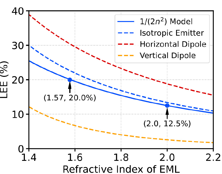
and are the fractions of total radiation sent directly into the upper escape cone. Figure 3 further assumes a phase-free, lossless perfect back reflector, so the identical downward-radiated fractions are redirected upward and the geometric outcoupling efficiencies become
and are the horizontal- and vertical-dipole light-extraction efficiencies predicted by this geometric model; light-extraction efficiency is abbreviated as LEE, and the superscript denotes the approximation. Without the ideal back reflector, both results are halved. An isotropic orientation ensemble contains two horizontal degrees of freedom and one vertical degree of freedom, so
Substitution of the preceding expressions reduces the isotropic result to
When is small, a first-order expansion of the square root gives
For air, , producing the solid blue curve in the figure. It is an approximation to the isotropic geometric result, not a separate law of emission. At , the horizontal, vertical, exact isotropic, and approximate values are about , , , and , respectively. Differences between the orientation curves arise from the dipole radiation patterns; their common decline comes from the narrowing escape cone at higher refractive index.
Wave-Optical Model of an OLED
A real OLED violates all of the assumptions above: its layer thicknesses are comparable to the wavelength; reflection has wavelength-dependent amplitude and phase; electrodes and functional layers absorb; guided and SPP states exist outside the escape cone; and the reflected field returns to the dipole and changes its total electromagnetic decay rate through the Purcell effect.
Dreapex TMM decomposes a dipole of orientation over normalized in-plane wavevector and calculates the complex amplitude of every component through the complete stack. When power is normalized to total radiation in a homogeneous reference environment, the total electromagnetic dissipation and target outcoupling efficiency are
Here, denotes horizontal or vertical orientation; is vacuum wavelength; is the dipole position in the EML; , where is in-plane wavevector and is vacuum wavenumber; is normalized total dissipated-power density per unit , while is the power density transmitted through the complete stack and across the target external boundary; is the orientation-dependent Purcell factor, or total electromagnetic decay relative to a homogeneous reference environment; is the interval associated with the target external-medium light cone; and is the fraction of electromagnetic-channel power that actually crosses the target external boundary.
Both power densities come from the same layered dipole field, which includes microcavity interference, Fresnel reflection and transmission, material absorption, waveguiding, and SPP coupling. is no longer fixed at 1, showing that the layered environment changes both energy partition and total dipole decay. Figure 3 contains no , , layer thickness, complex refractive index, or reflection phase, so it cannot model an OLED quantitatively.
Orientation Distribution
An isotropic orientation ensemble contains two orthogonal horizontal degrees of freedom and one vertical degree of freedom, giving
Here, is the power density of a dipole ensemble with isotropic orientation, is the mean power density of horizontal dipoles, and is the power density of vertical dipoles. The weights and arise from the three-dimensional orientation degrees of freedom; they do not mean that each molecule has three simultaneous dipole axes.
Using the vertical-dipole fraction for an arbitrary uniaxial orientation distribution,
Here, is the ensemble power density; is fully horizontal, is fully vertical, and is equivalent to isotropic orientation. The commonly reported horizontal-dipole ratio is . Molecular shape, substrate temperature, and deposition kinetics can all change this ratio.
Emission Position and Spatial Distribution
Dipoles with the same orientation see different reflection phases and near-field environments at different depths in the EML. A single position suits a narrow recombination zone; a broader zone requires a normalized distribution :
Here, and are the EML boundaries, is the dipole probability density through the layer thickness, is target-channel power, , or another single-dipole result at position , and is the spatial average. Point, exponential, Gaussian, and custom-file sources are different forms of .
Approaching a reflector changes the interference phase; approaching a metal also strengthens evanescent coupling. EML thickness alone therefore does not fully define the source—the location of the recombination zone inside that layer matters as well.
Applicability Conditions
| Condition | Meaning in the model | Consequence when violated |
|---|---|---|
| The emission center can be treated as a point dipole | Its size and charge-separation scale are much smaller than the wavelength | Higher multipoles or a nonlocal source model may be required |
| Layers are laterally uniform and much wider than a wavelength | Optical properties vary only with depth and edges do not enter the solution | Pixel edges, patterned electrodes, and scattering structures generally require a 3D model; a 2D cross section extrudes a point dipole into a line source and applies only when the geometry and source are translationally invariant along the omitted direction |
| Interfaces are flat with abrupt transitions | In-plane wavevector is conserved throughout the stack | Roughness mixes different in-plane wavevectors through scattering |
| The EML is coherent and transparent | The EML extinction coefficient is zero, so self-absorption is not calculated | Strong emission–absorption overlap leads to underestimated reabsorption and re-emission |
| Materials are linear, passive, and approximately nonmagnetic | Complex refractive indices do not depend on field strength, and permeability is 1 | High-intensity, gain, or magneto-optic media require an extended model |
| Anisotropy is uniaxial with the optical axis normal to the layers | In-plane rotational symmetry remains, allowing ordinary and extraordinary responses to be separated | Tilted-axis, in-plane-oriented, or biaxial materials lie outside the model |
| The outcoupling-side external medium is transparent | Its light cone and the top outcoupling channel have a clear physical meaning | An absorbing outer boundary cannot be defined as an outcoupling channel |
Additional notes on the condition that layers are laterally uniform and much wider than the wavelength:
- For a laterally uniform planar device, a 1D model is generally more accurate than FDTD.
- The present model assumes laterally infinite layers. The 1D design remains valid above
1 μmpixel width; edge effects must be considered at1 μmor below. Jung et al. (2026)
Finite metals and other absorbing layers may remain inside the device; their energy is assigned to absorption or evanescent channels. A bottom-outcoupled channel exists when the bottom external medium is transparent; it is zero for an absorbing bottom boundary.
Next Step
Continue with Microcavity Effect to see how reflecting interfaces transform the same dipole source into different spectra, colors, and angular distributions.
Reference
- Novotny, L.; Hecht, B. Principles of Nano-Optics. Cambridge University Press, 2012.
- Griffiths, D. J. Introduction to Electrodynamics, 4th ed.; 2021.
- Marcato, T.; Shih, C. J. Molecular Orientation Effects in Organic Light-Emitting Diodes. Helv. Chim. Acta 2019, 102. https://doi.org/10.1002/hlca.201900048
- Wasey, J. A. E.; Barnes, W. L. Efficiency of Spontaneous Emission from Planar Microcavities. J. Mod. Opt. 2000, 47, 725–741.
- Yokoyama, D. Molecular Orientation in Small-Molecule Organic Light-Emitting Diodes. J. Mater. Chem. 2011, 21, 19187–19202.
- Chance, R. R.; Prock, A.; Silbey, R. Molecular Fluorescence and Energy Transfer near Interfaces. Adv. Chem. Phys. 1978, 37, 1–65.
- Jung, D.; Cho, H.; So, Y.; Cho, C. Optical Modeling of Top-Emitting Micro-OLEDs. Macromol. Res. 2026. https://doi.org/10.1007/s13233-026-00533-8