SPP Mode Suppression in an Inverted Single-Layer OLED
Inverted device architecture for high efficiency single-layer organic light-emitting diodes with imbalanced charge transport
Authors: Xiao Tan, Dehai Dou, Lay-Lay Chua, Rui-Qi Png, Daniel G. Congrave, Hugo Bronstein, Martin Baumgarten, Yungui Li, Paul W. M. Blom, and Gert-Jan A. H. Wetzelaer
Journal: Nature Communications 15, 4107 (2024) · Comparison target: Figure 4b · License: CC BY 4.0
An 80 nm layer of blue-emitting material reaches only 10% outcoupling in a conventional device: the recombination zone sits against the metal cathode, and most of the power is taken by surface-plasmon-polariton (SPP) modes. Replace that cathode with a transparent electrode on the glass side, the recombination zone moves away from the metal, and outcoupling doubles to 20%.
This case uses the published emitter optical constants, dipole orientation, and recombination profile to build a conventional and an inverted model, runs Power Dissipation for the spectra of paper Figure 4b, then uses Mode for the channel integrals.
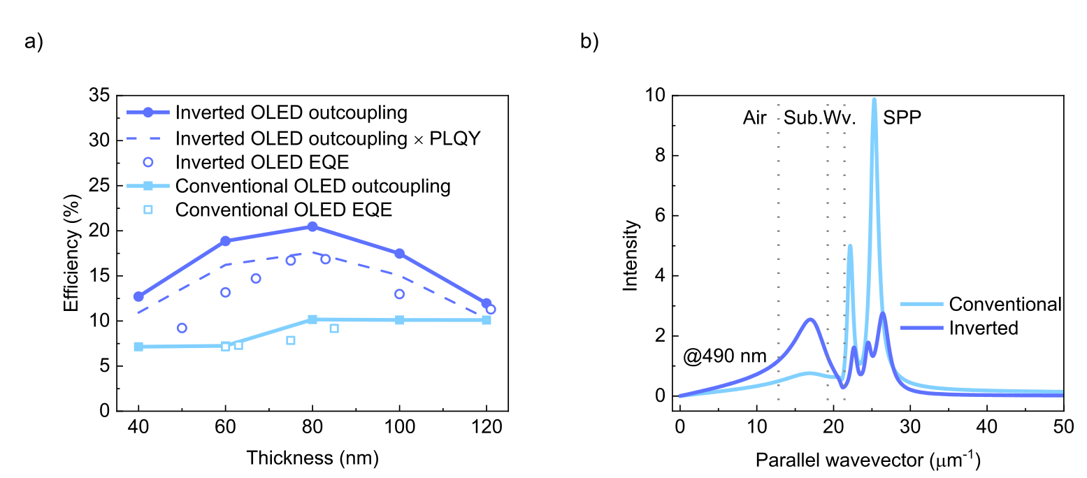
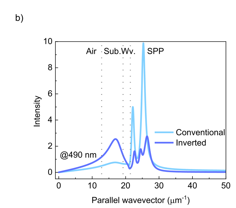
The light-blue curve in Figure 4b has a sharp SPP-region peak of about 10.35, whereas the inverted dark-blue curve peaks at about 2.77; Figure 4a also provides outcoupling anchors of 10.15% and 20.47% at 80 nm.
Background
In a planar OLED, emitting dipoles can couple power into air, the glass substrate, organic waveguide modes, and SPP modes at the metal interface. Figure 4b separates these channels by in-plane wavevector. To map the published Source Data directly to the dimensionless Dreapex TMM axis, this case converts the in-plane wavevector to effective index:
Here, is the effective index, is the wavevector parallel to the layers, is the vacuum wavenumber at wavelength , and is the circle constant. This case fixes . The three published boundaries become 1.00, 1.50, and 1.67, matching the light lines of air, the glass substrate, and the 2tCz2CzBN emissive layer.
The Power Dissipation spectrum retains peak positions and modal density. Mode integrates that spectrum across in-plane wavevector into outcoupling, substrate, waveguide, absorption, and evanescent channels. Together, they show whether inversion genuinely moves power away from the high-wavevector loss region.
Structure
Both stacks run from the glass emission side to the top metal. The tables use for the real part of the refractive index and for the extinction coefficient.
Conventional device
| Layer | Thickness | Optical input |
|---|---|---|
| Glass, incoherent | 1 mm | , constrained by the Figure 4b substrate boundary |
| ITO | 100 nm | Open thin-film optical data; fixed thickness assumption |
| PEDOT:PSS | 40 nm | Open measured optical data |
| MoO₃ | 7 nm | Open measured thin-film optical data |
| C₆₀ optical proxy | 4 nm | , |
| 2tCz2CzBN EML | 80 nm | Continuous measured from Figure S4c; the emissive layer is entered with an extinction coefficient of 0, which never enters the emission solve |
| TPBi | 4 nm | Quartz-film data from the open Aulika et al. dataset |
| Ba effective layer | 5 nm | Open optical data for the adjacent Al |
| Al cathode | 100 nm | Open measured Al optical data |
Inverted device
| Layer | Thickness | Optical input |
|---|---|---|
| Glass, incoherent | 1 mm | |
| ITO | 100 nm | Same as the conventional device |
| n-TFB optical proxy | 14 nm | Neutral TFB at 490 nm: , |
| TPBi | 4 nm | Same as the conventional device |
| 2tCz2CzBN EML | 80 nm | Continuous measured from Figure S4c; that data has at 490 nm, and the emissive layer is entered with an extinction coefficient of 0 |
| C₆₀ optical proxy | 4 nm | , |
| MoO₃ | 10 nm | Same data source as the conventional device |
| Al anode | 100 nm | Same data source as the conventional device |
Layer order and thicknesses follow SI Table 1. The Methods section gives 45 nm for PEDOT:PSS, while SI Table 1 and the supporting captions used for the figures give 40 nm; the primary model uses the latter. The paper does not report the ITO thickness or publish sample-matched optical constants for the auxiliary layers. Both devices therefore use the same open datasets and proxies fixed before running, leaving layer order and recombination-profile direction as the comparison variables. The n-TFB proxy is the TFB value extracted from the open Miao et al. 2020 paper.
Once entered, the conventional structure page looks like this. The 5 nm Ba layer keeps its geometrical thickness, with its optical input labelled explicitly as an effective Al proxy:

The inverted device puts the cathode on the glass side, replaces PEDOT:PSS and MoO₃ with n-TFB, and turns the top metal into the anode:

Optical and Emitter Settings
All emitter inputs come from the paper's Source Data, and both models share the same values.
| Emitter setting | Value |
|---|---|
| Wavelength | 490 nm, single wavelength |
| Vertical-dipole fraction | 0.254; Custom orientation |
| Spatial distribution | The complete 51-point recombination array published for 3.0 V and an 80 nm EML |
| Spectral convention | Unit White, Probability; no additional spectral weighting in a single-wavelength run |
| Quantum and conversion efficiencies | Both 1, for normalized optical-channel comparison |
12 nm, this case interprets the coordinate as distance from the cathode. The cathode is on the top-metal side in the conventional device, so the imported position is ; it is on the glass side in the inverted device, so the imported position is . Mirroring the same electrical recombination profile into the two physical electrode directions is the main structural variable of this case.In the conventional device the emission zone peaks next to the top metal cathode:

The inverted device uses the same 51 density samples with the coordinate reversed, so the peak sits next to the bottom transparent cathode:

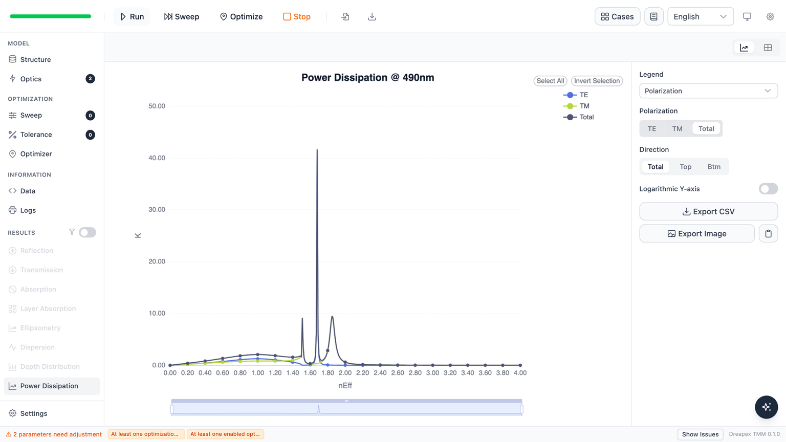
Both detectors are enabled at 490 nm in Single mode. For Power Dissipation, select nEff on the horizontal axis with a range of 0–4 and a 0.01 step; the comparison curve is for Total polarization and Total direction, the power coupling coefficient summed over all polarizations and both propagation directions:

Mode integrates the same calculation across in-plane wavevector to give the channel fractions:

Optimize. If a notice related only to Optimize appears at the bottom of the page, continue with Run.Simulation Results and Comparison with Figure 4
The thickness dependence in panel a is out of scope here: it needs a recombination profile for each of the 40, 60, 100, and 120 nm devices, and the paper publishes a profile only for the 80 nm device.
Power-dissipation spectra
Published panel b:
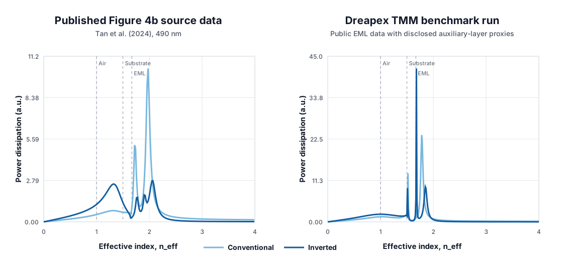
The paper publishes numerical source data for this figure, plotted here against this run on the same nEff axis:
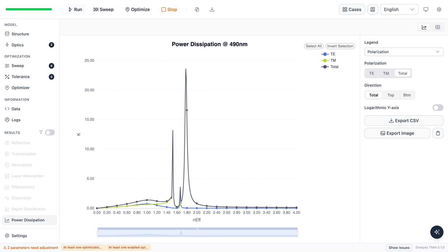
The raw results in the app. The conventional device has a tall peak in the SPP region:
In the inverted device the same region keeps only about four tenths of that height:
| Quantity | Paper conventional | Paper inverted | Simulation conventional | Simulation inverted |
|---|---|---|---|---|
| SPP peak | 1.9768 | 2.0684 | 1.78 | 1.85 |
| SPP peak height | 10.3451 | 2.77122 | 23.6221 | 9.50531 |
Integral over 1.67–4 | 2.09225 | 0.86106 | 2.24522 | 1.55935 |
The inverted/conventional peak-height ratio is 0.4024 here and the SPP-region integral ratio 0.6945, against 0.268 and 0.412 in the paper: both datasets show inversion cutting high-wavevector loss to less than half, and both move the peak to higher . Peak detection starts at 1.70 to exclude the narrow light-line boundary feature near the EML; the integral still starts at 1.67 and includes it.
Channel integrals
Published panel a, outcoupling efficiency against emissive-layer thickness:
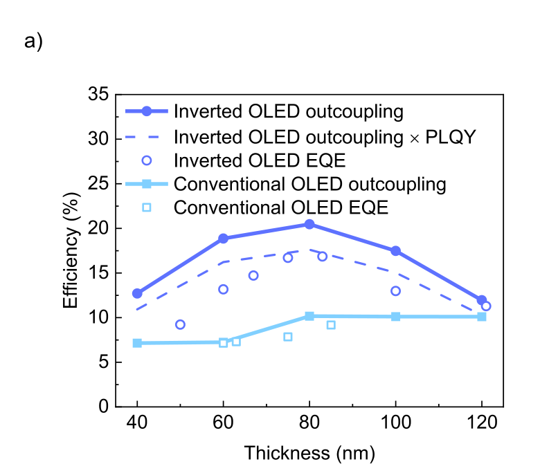
At 80 nm the paper gives 10.15% conventional and 20.47% inverted. Switching the same pair of models to the Mode detector and reading the Top Outcoupling channel:
Outcoupling efficiency (the same 80 nm emissive-layer device) | Conventional | Inverted | Inverted / conventional |
|---|---|---|---|
| Paper Figure 4a, integrated over the device emission spectrum | 10.15% | 20.47% | 2.02 |
This run, Mode at a single wavelength of 490 nm | 10.84% | 25.27% | 2.33 |
This run, Mode averaged flat over 450–560 nm | 10.22% | 23.96% | 2.34 |
The paper integrates the full emission spectrum while Figure 4b is drawn explicitly at 490 nm, which is why the primary comparison uses 490 nm. How much the spectral weighting is worth can simply be measured: switching the Mode wavelength mode to a 420–650 nm sweep puts the Top Outcoupling maximum of both devices near 490–500 nm, falling away slowly on either side, and the paper's measured emission peak λ_EL is also 490 nm. Averaging flat across the emission band moves the conventional device from 10.84% to 10.22% and the inverted one from 25.27% to 23.96%, leaving the ratio at 2.33. Narrowing the window to 460–540 nm or 470–520 nm keeps the ratio between 2.33 and 2.34.
The single-wavelength versus spectrally integrated distinction is therefore worth at most 1.3 percentage points, which does not account for the 4.8 percentage-point gap to the paper on the inverted device. That comes from the input differences described below.
The raw Mode results show where the ratio comes from. The conventional device puts 68.62% of its power in the Evanescent channel — the SPP peak of the power-dissipation spectrum above:

The inverted device drops Evanescent to 42.92%, and most of the released power goes into Top Outcoupling and Substrate:

Deviation Notes
The paper publishes continuous only for the 2tCz2CzBN emissive layer, not sample-matched data for the auxiliary layers. ITO, PEDOT:PSS, MoO₃, TPBi, and Al use open measurements; n-TFB, C₆₀, and Ba use the proxies listed above; and the ITO thickness, which is not reported, is fixed at 100 nm. The differences in SPP peak position and absolute height come mainly from this set of input differences. Both stacks share the same inputs, so nothing here creates an artificial inversion advantage.
The paper does not state which voltage-dependent recombination profile Figure 4b uses, nor the origin and direction of its position coordinate. This case freezes the published 3.0 V curve and interprets the coordinate as distance from the cathode, from the paper text and the peak location.
The planar model excludes roughness, lateral scattering, edge emission, and electrode morphology, all of which redistribute high-wavevector power.