Why Does the Optimized a-Si Cell Absorb More Light? Electric Field, Energy Flow, and Absorption Density
This tutorial continues Which Layer Absorbs the Light? Analyze and Optimize an a-Si Thin-Film Solar Cell, using the same baseline design, optimized design, and normal incidence at 550 nm.
The previous tutorial showed that optimization raises the a-Si absorption at 550 nm from 91.096% to 96.496%. Here we look inside the layers and use electric field, energy flow, and absorption density to explain where that gain comes from. By the end, you can turn one absorptance value into a spatial account of where light is enhanced, how it travels, and where it is dissipated.
Meaning of the Depth Results
Depth starts at the incidence-side surface and proceeds through ITO and a-Si. The three results have distinct roles:
| Result | Main information | Use in this tutorial |
|---|---|---|
Electric Field | Local field variation with depth | Locate standing-wave nodes, antinodes, and field-enhanced regions |
Poynting Vector | Change in net forward energy flow | Find where energy falls rapidly and how much reaches the back of the structure |
Absorption Density | Local optical loss per unit depth | Locate where optical power is actually dissipated |
An electric-field maximum is not automatically an absorption maximum. A local field produces absorption only where the material has a nonzero extinction coefficient. In a lossy layer the Poynting flux decreases continuously, and the lost flux is the power absorbed by the material.
Fix the Structures and Optical Conditions
Compare the two structures from the previous tutorial without changing the materials or wavelength:
| Design | ITO | a-Si | Total absorptance at 550 nm |
|---|---|---|---|
| Baseline | 80 nm | 200 nm | 91.096% |
| Optimized | 62.372 nm | 485.857 nm | 96.496% |


On the Optics page, select 550 nm, 0° incidence, and unpolarized light. Enable Electric Field, Poynting Vector, and Absorption Density, then set the depth resolution to 2 nm.

Use the same wavelength and depth resolution for both structures so their spatial distributions remain directly comparable.
Light Propagation in the Baseline Design
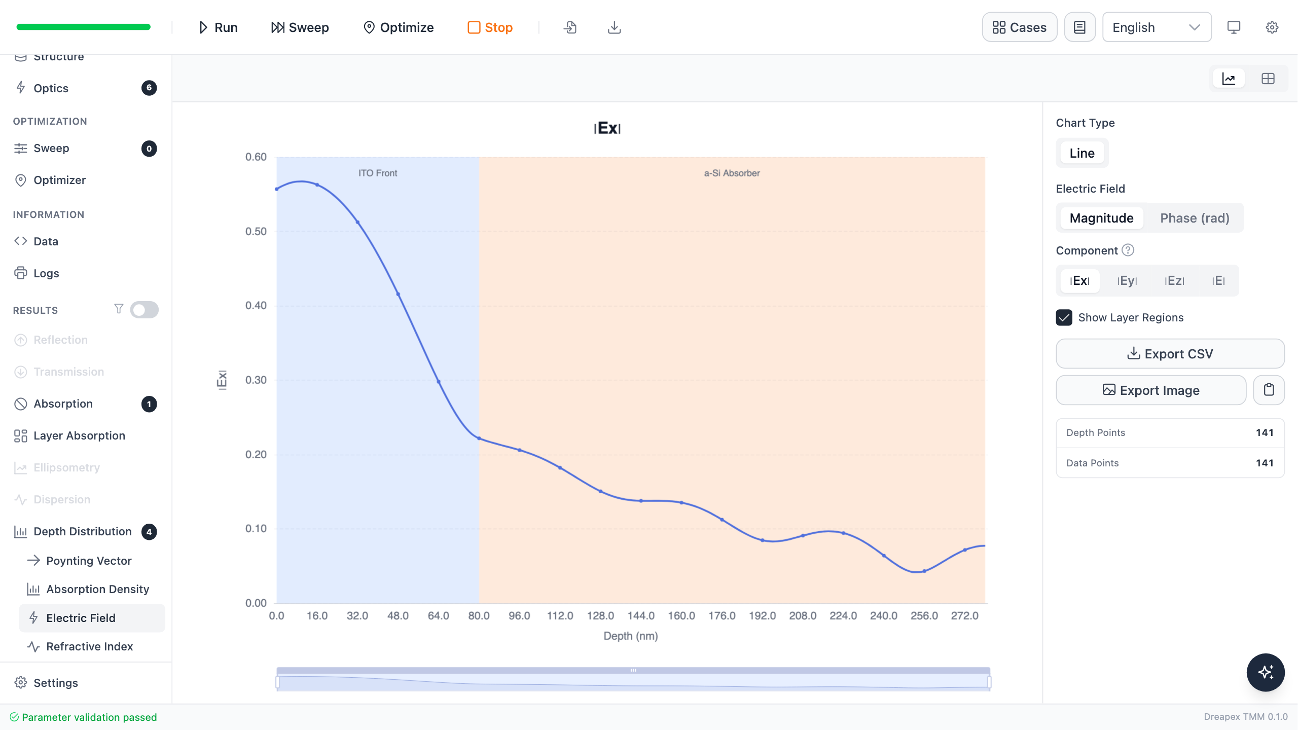
The field oscillates strongly near the ITO/a-Si interface, then decays through a-Si. This curve shows how interference redistributes the local field, but it cannot by itself tell how much power is absorbed at each position.
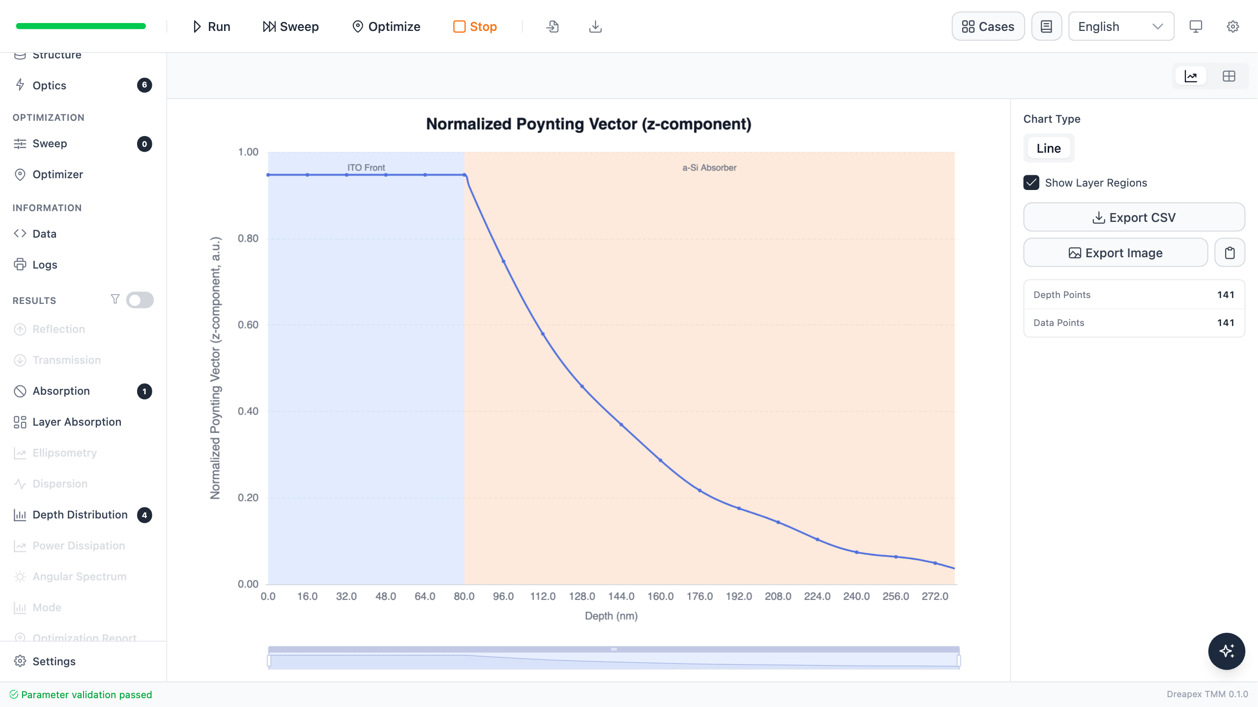
The normalized net flux is about 0.947 at the front of a-Si and about 0.036 after 200 nm of a-Si. Its continuous decline inside a-Si directly shows the active layer absorbing optical power.
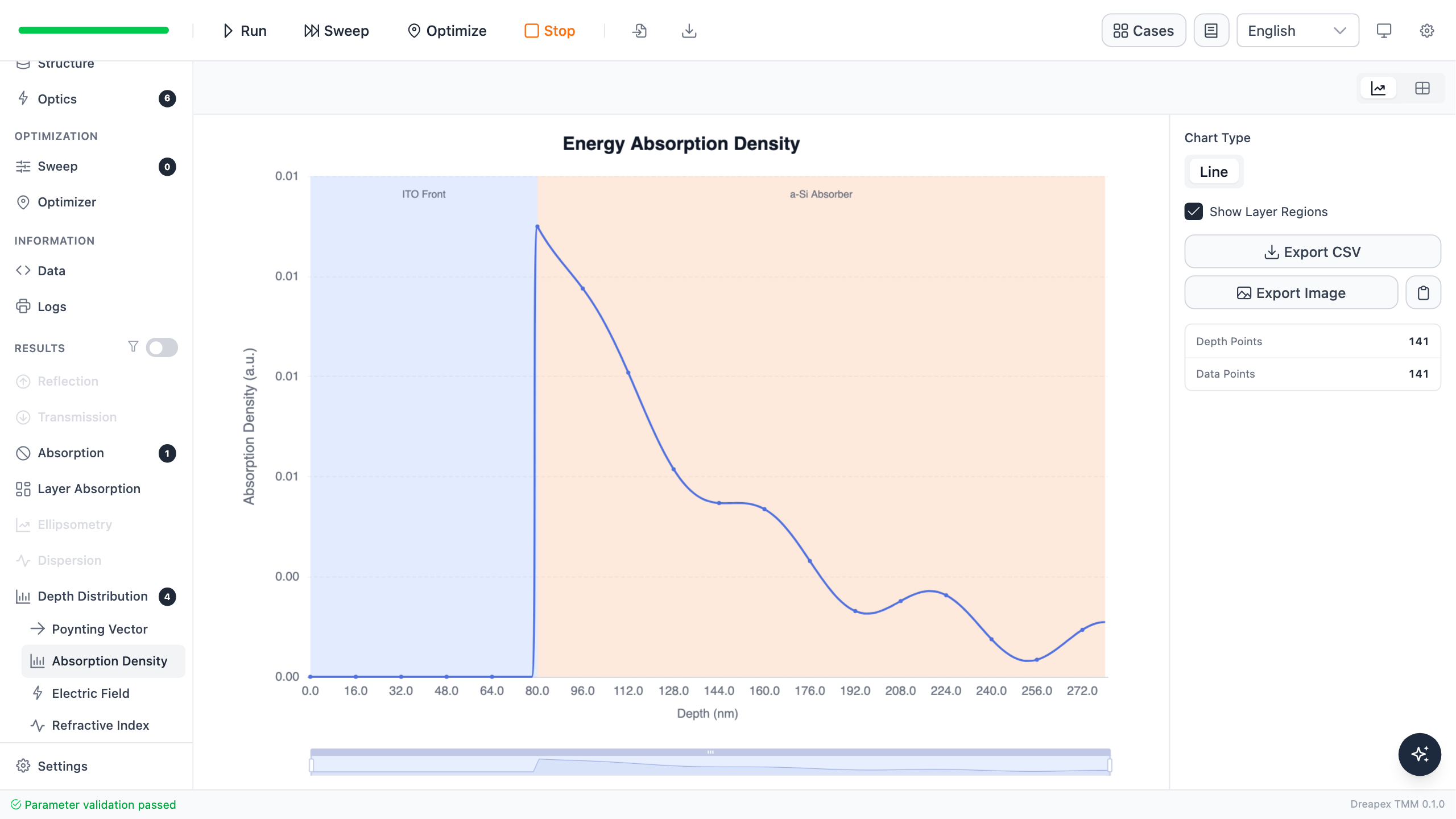
Absorption is concentrated near the front of a-Si, with a maximum of about 0.01349 a.u. The local absorption falls deeper in the layer as the field and energy flow decay.
The Optimized Design Extends Absorption Deeper
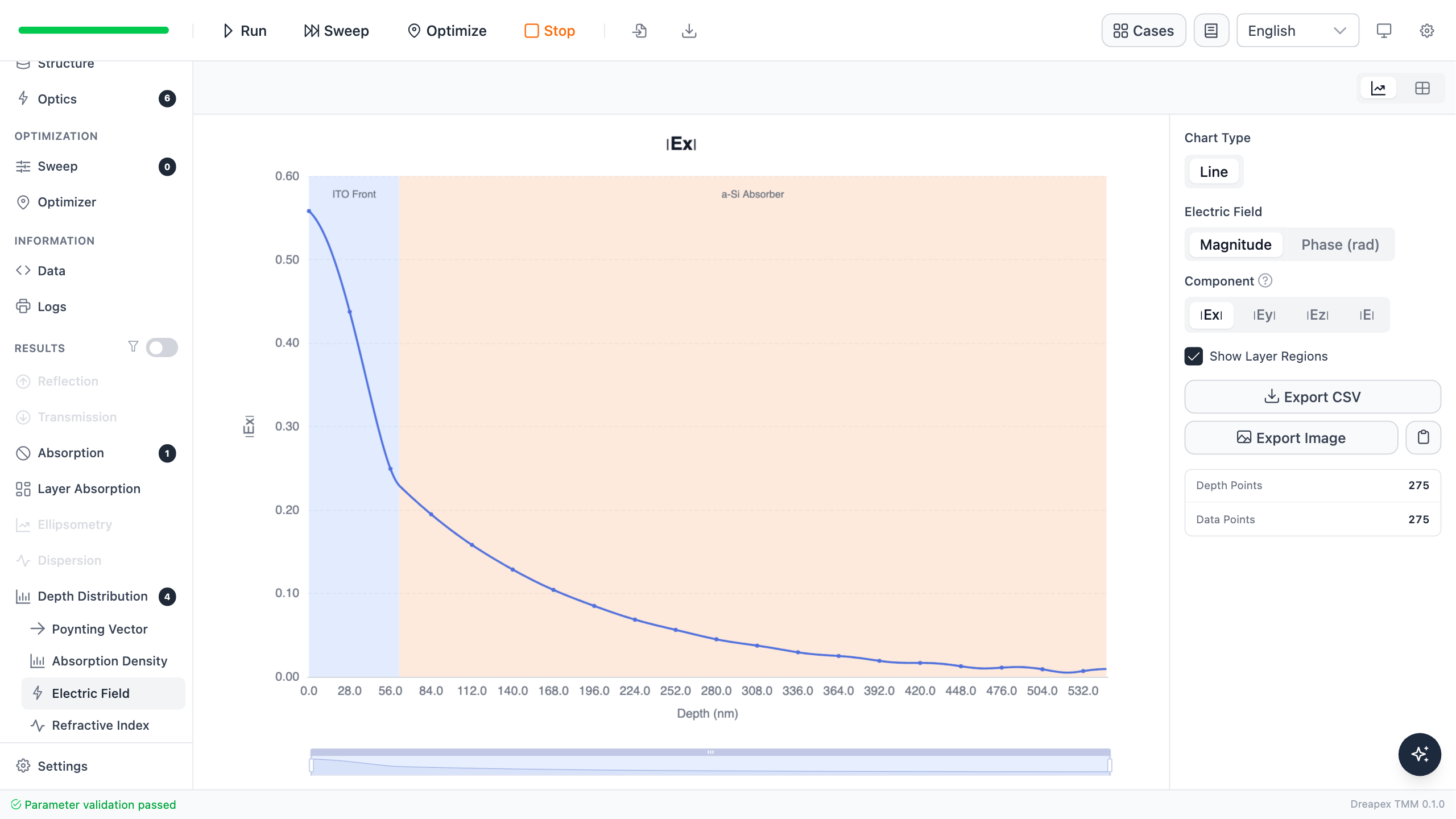
The optimized a-Si is thicker, so the field passes through more oscillations while decaying across the active layer. The thickness change also alters the interface phase condition; the new curve is not a simple horizontal stretch of the baseline result.
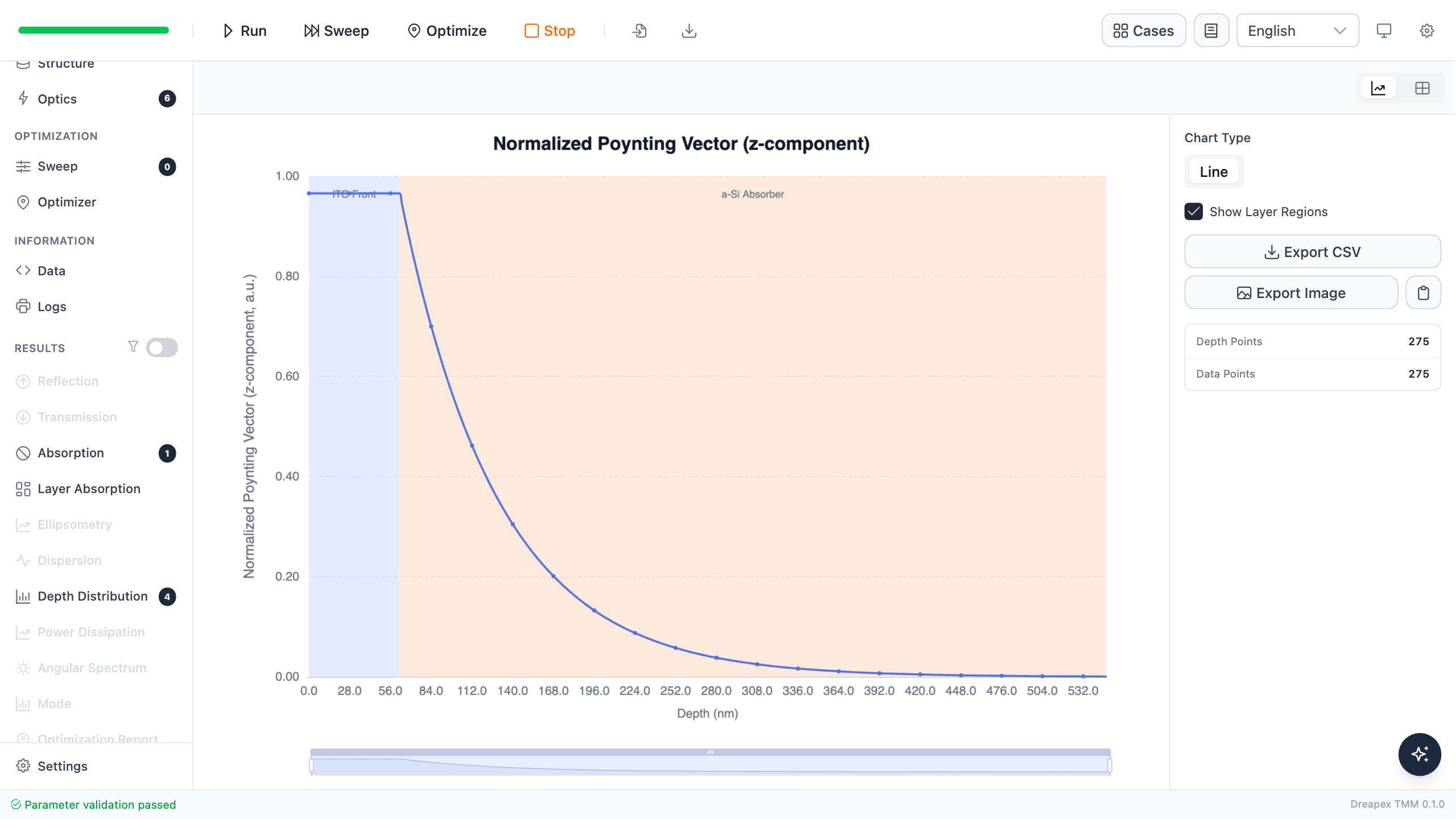
The normalized net flux is about 0.965 at the front of a-Si and only about 0.00054 at its back surface. Compared with the baseline, much more energy has been dissipated in a-Si before light reaches the glass.
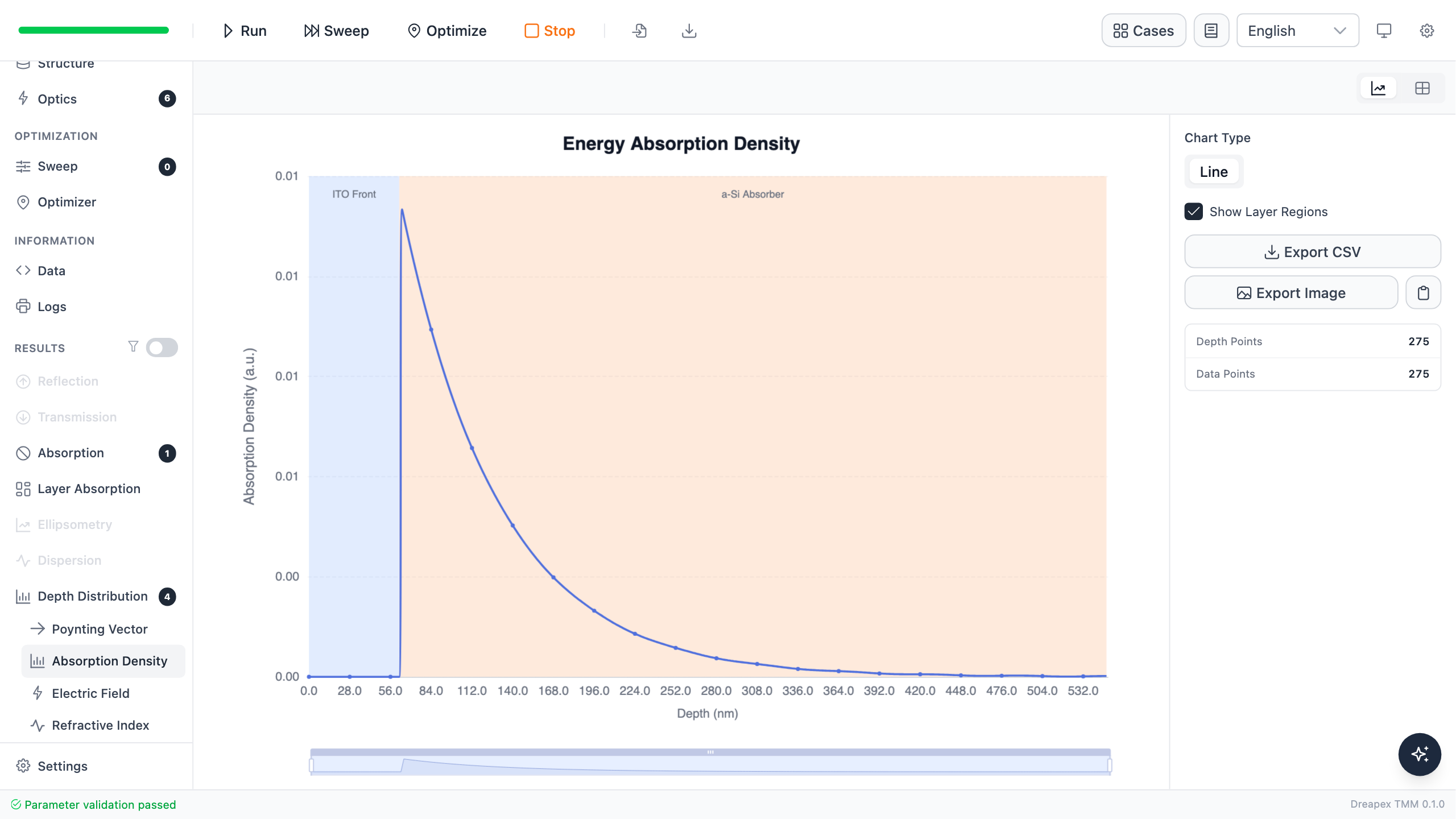
The absorption-density maximum is about 0.01400 a.u., only slightly above the baseline maximum. The important change is that the absorbing region extends from 200 nm to almost 486 nm. Most of the gain comes from a longer effective absorption path, not from a sudden increase at one local peak.
Explain the Gain with Spatial Evidence
| Metric at 550 nm | Baseline | Optimized | Interpretation |
|---|---|---|---|
| a-Si thickness | 200 nm | 485.857 nm | Longer effective absorption path |
| Total absorptance | 91.096% | 96.496% | More incident power dissipated in the stack |
| Net flux at a-Si front | About 0.947 | About 0.965 | More energy enters the active layer |
| Net flux at a-Si back | About 0.036 | About 0.00054 | Almost no energy remains after the active layer |
| Maximum absorption density | About 0.01349 a.u. | About 0.01400 a.u. | Similar peak, much longer absorbing region |
R/T/A tells us how much absorption increased; depth distributions explain why. In this example, thinner ITO improves optical coupling and thicker a-Si lengthens the absorption path. Together they reduce reflection and residual transmission, allowing the energy flow to decay more completely in the active layer.
This remains an optical conclusion. Stronger fields and higher optical absorption do not by themselves establish a higher solar-cell conversion efficiency; a real device also depends on carrier recombination, transport, and electrode losses.
Variation Exercise
Keep ITO at 62.372 nm and change a-Si to 300 nm. Run the 550 nm depth distributions, compare the net flux at the a-Si back surface and the maximum absorption density, then decide whether the lower absorption comes mainly from a weaker local field or a shorter effective path.
← Back to Tutorial Catalog · Next: Effect of a Fabry–Pérot Filter on a Short Pulse