Which Layer Absorbs the Light? Analyze and Optimize an a-Si Thin-Film Solar Cell
For a thin-film solar cell, absorption by the whole stack does not necessarily contribute to photoconversion: only light absorbed in the active a-Si layer can participate, while absorption in ITO is a parasitic loss.
This tutorial uses a simplified ITO/a-Si structure to identify which layer absorbs the light. You will use R/T/A and Layer Absorption to separate active-layer absorption from parasitic absorption, then improve average a-Si absorption over 400–700 nm with a thickness sweep and optimization.
Distinguish Active-Layer and Parasitic Absorption
Amorphous silicon (a-Si) is the active absorber in this model. ITO is the transparent front electrode; light absorbed by ITO is usually a parasitic loss and should not be treated as a-Si absorption.
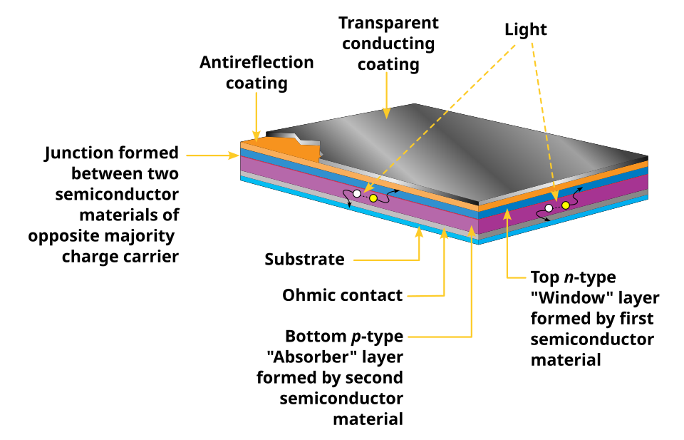
This tutorial simplifies the transparent conducting layer as ITO and the absorber as a-Si. The layer-absorption result then separates parasitic ITO loss from useful a-Si absorption.
The complex refractive index of an absorbing material is
Here, is the complex refractive index, is its real part, is the extinction coefficient, is the imaginary unit, is the absorption coefficient, and is the vacuum wavelength. A larger makes light decay more rapidly inside the material. Interference also changes the electric-field distribution within a thin-film stack, so layer absorption cannot be inferred from thickness alone.
At every wavelength, a passive stack satisfies
Here, , , and are power reflectance, transmittance, and total absorptance, respectively; is the fraction of incident power absorbed in layer ; and is the number of layers. Absorptance gives the total absorption, while Layer Absorption answers the more useful question: “Which layer absorbs the light?”
The same distinction applies to photodetectors, selective absorbers, and light-emitting devices. Absorption in the target layer is usually useful, whereas absorption in an electrode or package is often a loss.
Build a Simplified ITO/a-Si Structure
Build an air/ITO/a-Si/glass structure. Use the wavelength-dependent teaching data for ITO and a-Si from the case library, and set the bottom glass to a constant refractive index of 1.52.
| Position | Material | Thickness | Index type |
|---|---|---|---|
| Top medium | Air | — | Constant, , |
| Layer 1 | ITO | 80 nm | File |
| Layer 2 | a-Si | 200 nm | File |
| Bottom medium | Glass | — | Constant, , |

This model is intended for learning optical absorption allocation. It omits the back electrode, doped layers, texture, and carrier transport, so its results are not solar-cell conversion efficiency.
Set the Optical Conditions
On the Optics page, set 400–900 nm with a 5 nm step, 0° incidence, and unpolarized light. Enable Reflectance, Transmittance, Absorptance, and Layer Absorption.
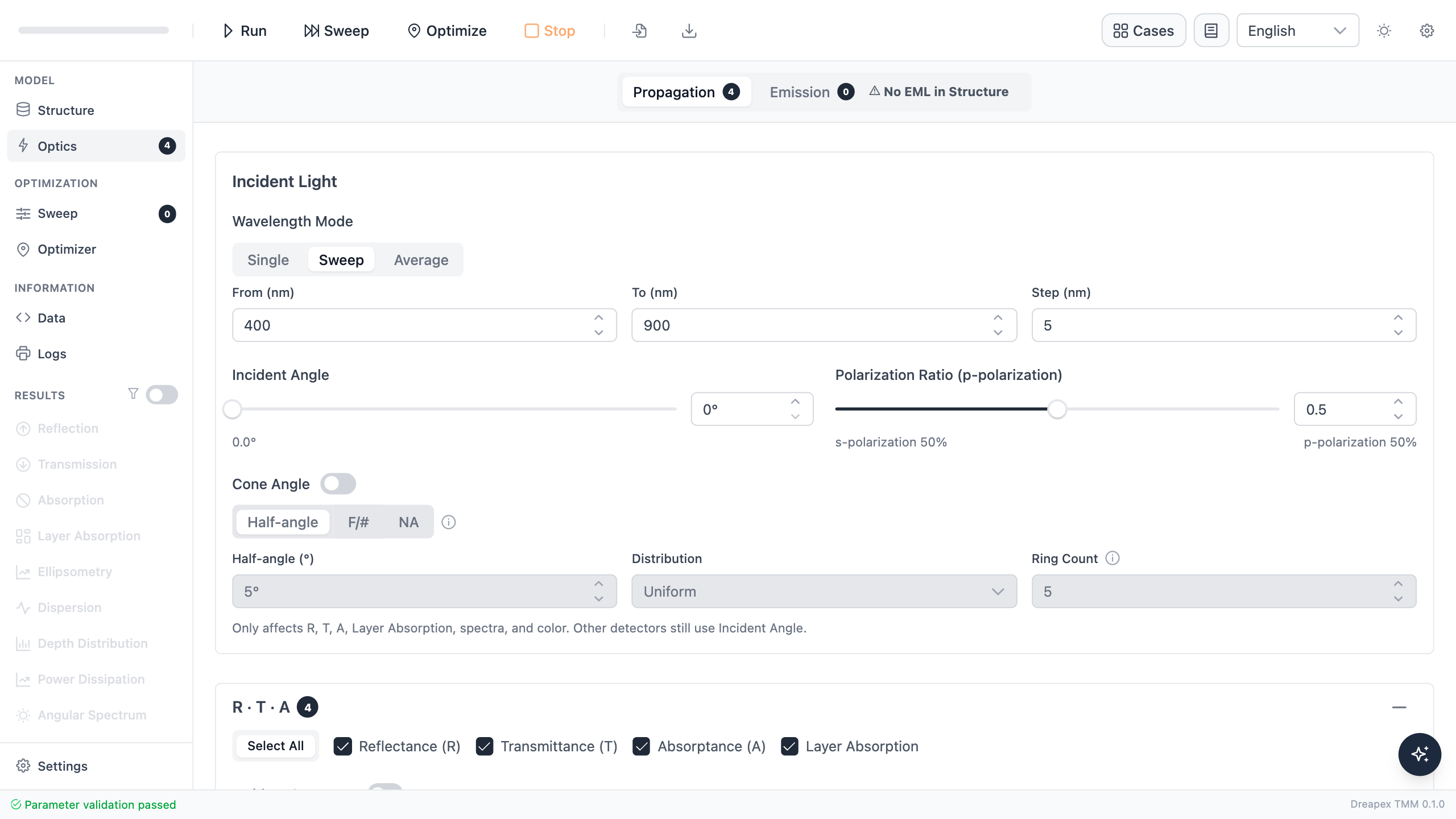
The 400–900 nm range reveals the a-Si absorption edge; the design metric below is evaluated only from 400–700 nm. When no incident spectrum is enabled, a band average is the arithmetic mean of the sampled wavelengths, not a solar-spectrum-weighted efficiency.
Establish an Absorption Baseline
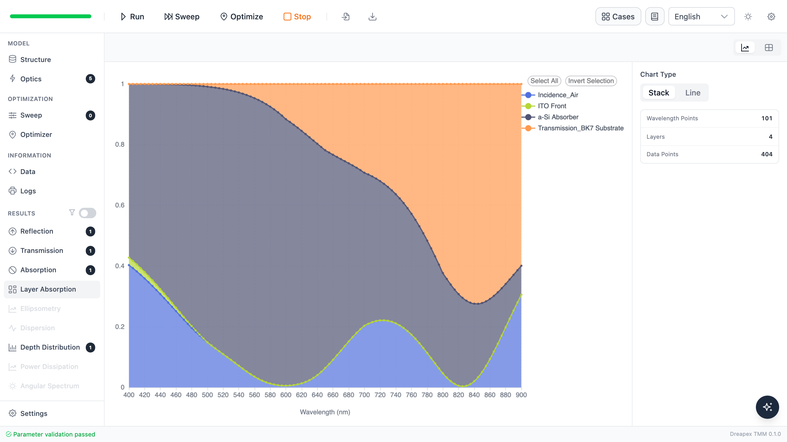
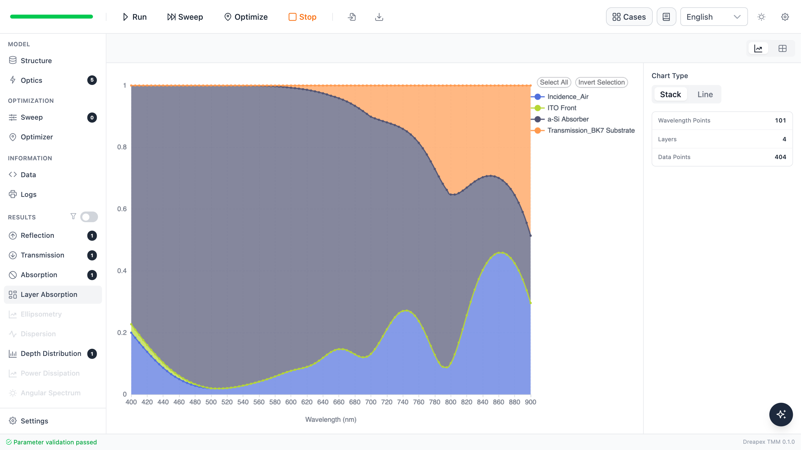
Run the calculation, verify R/T/A first, and then open Layer Absorption.
| Condition | Total | ITO absorption | a-Si absorption | ||
|---|---|---|---|---|---|
| 400–700 nm average | 14.217% | 8.672% | 77.110% | 0.461% | 76.650% |
| 550 nm | 5.269% | 3.635% | 91.096% | 0 | 91.096% |
Total absorption agrees with the sum of the two layer contributions, and the maximum energy-closure error across all wavelengths is approximately . Energy conservation confirms that the result is complete, but only the layer-resolved result shows whether the absorption occurs in a-Si.
Sweep the a-Si Thickness
In Sweep, select a-Si Absorber → Thickness and sweep from 100 nm to 500 nm in 50 nm steps. Keep the rest of the structure and all optical settings unchanged.

After selecting Sweep, open the Layer Absorption result and set Layer to a-Si Absorber. The nine curves correspond to a-Si thicknesses from 100 to 500 nm.
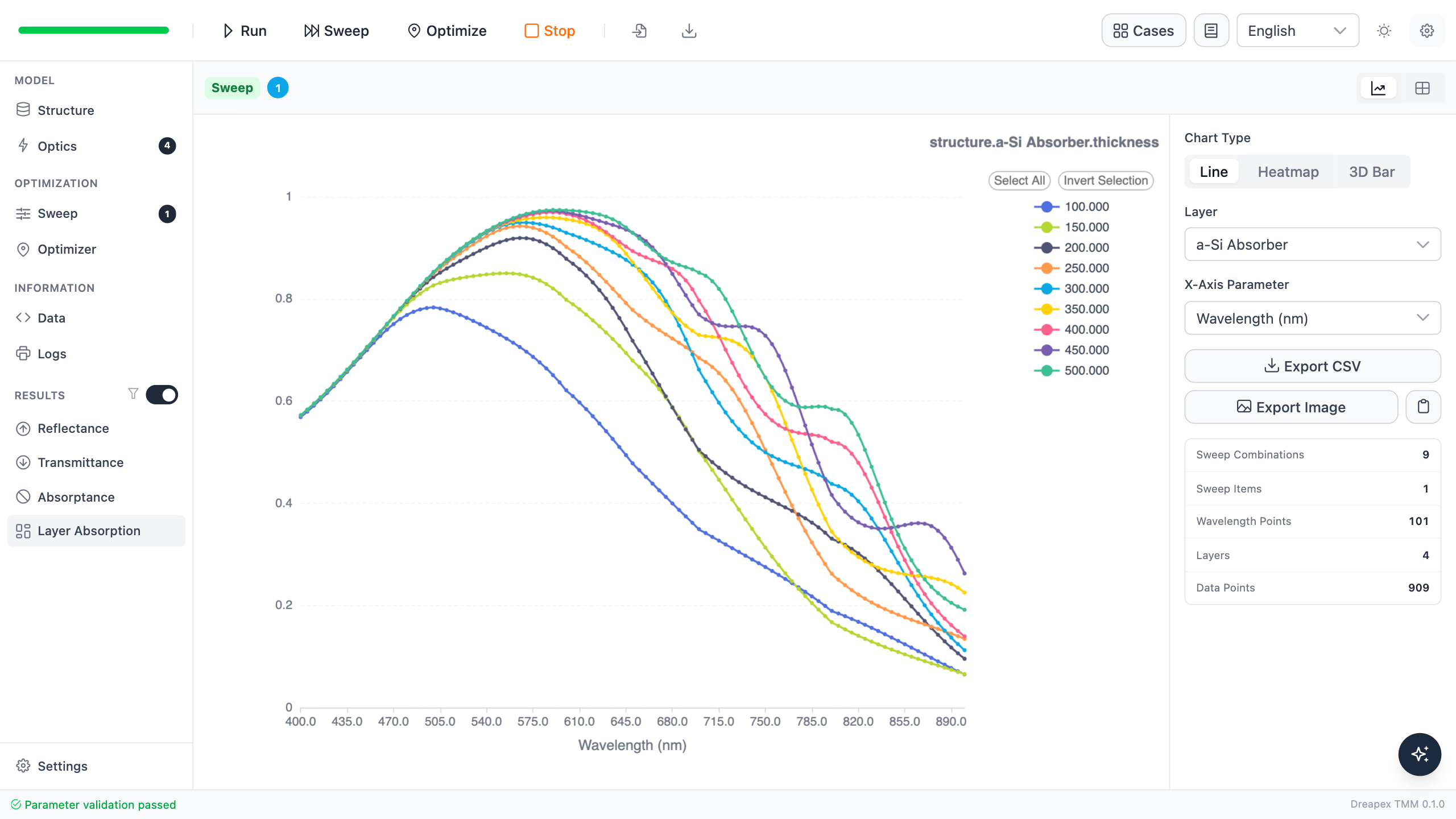
| a-Si thickness | Average | Average | Average a-Si absorption |
|---|---|---|---|
| 100 nm | 18.000% | 18.594% | 62.949% |
| 200 nm | 14.217% | 8.672% | 76.650% |
| 300 nm | 12.788% | 4.635% | 82.116% |
| 400 nm | 12.645% | 2.551% | 84.344% |
| 500 nm | 12.837% | 1.433% | 85.270% |
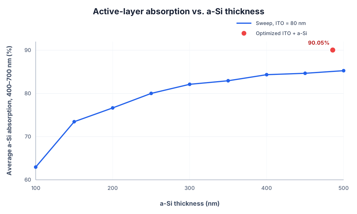
As a-Si thickness increases from 100 nm to 500 nm, average transmittance falls from 18.594% to 1.433% and active-layer absorption rises from 62.949% to 85.270%. Reflectance is not monotonic; it oscillates around 13% because interference redistributes the field inside the stack.
Optically, thicker a-Si absorbs more light. It also uses more material and may reduce carrier-collection efficiency. The thickness sweep reveals the optical trend, but it cannot determine the optimum thickness of a real cell by itself.
Optimize Active-Layer Absorption Directly
The objective is the average layer absorption of a-Si:
Here, is the average a-Si layer absorption; is the a-Si absorption at wavelength ; is the sample index; and is the number of samples from 400–700 nm at a 5 nm step.
In Optimizer, use the following settings:
| Item | Setting |
|---|---|
| Objective | Maximize the average a-Si Layer Absorption |
| Band | 400–700 nm, 5 nm step |
| Variable 1 | ITO thickness, 40–140 nm, starting at 80 nm |
| Variable 2 | a-Si thickness, 100–500 nm, starting at 200 nm |
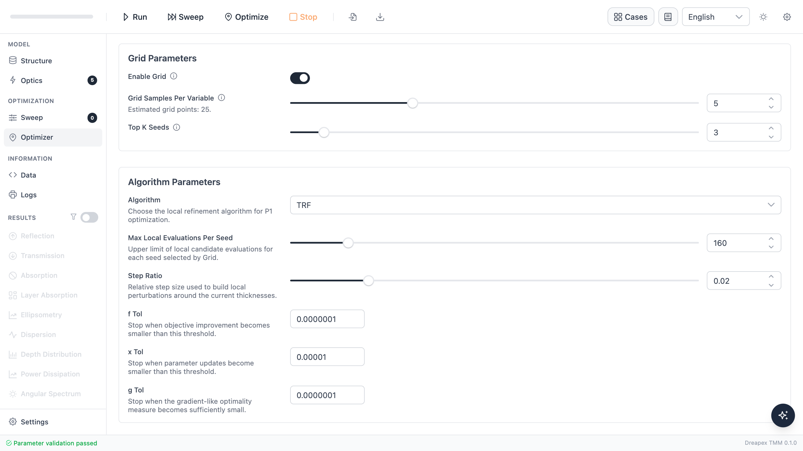
| Algorithm | TRF, up to 160 evaluations |
| Global starts | Grid 5 × 5, retain 3 seeds |

Do not substitute total Absorptance for this objective. An increase in total absorption could come from ITO, where the absorbed light never reaches the a-Si layer.
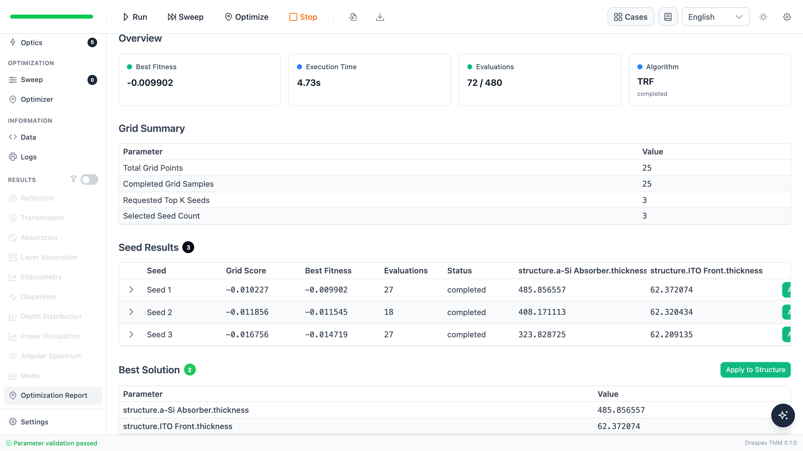
After 72 objective evaluations and 34 iterations, the optimizer finds an ITO thickness of 62.372 nm and an a-Si thickness of 485.857 nm. Select Apply to Structure, then return to Structure and confirm that the thicknesses have been updated.

Validate the Optimum with a Forward Calculation
After applying the optimum thicknesses, run the calculation again. Do not treat the optimization report itself as the final result.
| 400–700 nm average metric | Baseline | Optimized | Change |
|---|---|---|---|
| 14.217% | 8.052% | −6.165 percentage points | |
| 8.672% | 1.426% | −7.247 percentage points | |
| Total | 77.110% | 90.522% | +13.412 percentage points |
| ITO absorption | 0.461% | 0.473% | +0.012 percentage points |
| a-Si absorption | 76.650% | 90.049% | +13.399 percentage points |
Average a-Si absorption improves by 13.399 percentage points, or approximately 17.48% relative, while parasitic ITO absorption is nearly unchanged. At 550 nm, a-Si absorption is 96.496%, and the final result still satisfies .
The optimum a-Si thickness lies near the 500 nm upper bound, showing that this purely optical objective still favors a thicker absorber. An engineering design should add constraints for manufacturable thickness, material use, and electrical collection, and it should use weighting by a real solar spectrum.
Variation Exercise
In the current model, reset the a-Si thickness to 200 nm, then set the ITO thickness to 40, 80, and 120 nm in turn. Record the average ITO and a-Si layer absorption for each case, then determine whether any increase in total absorption actually reaches the active layer.
← Back to Tutorial Catalog · Next: Why Does the Optimized a-Si Cell Absorb More Light?