Your First Thin-Film Design: From Bare Glass to Broadband AR
Why does the left half of this lens show bright reflections while the right half almost disappears? The antireflection coating on the right does not block the light. It makes two reflected waves weaken each other, allowing more light to enter the lens.
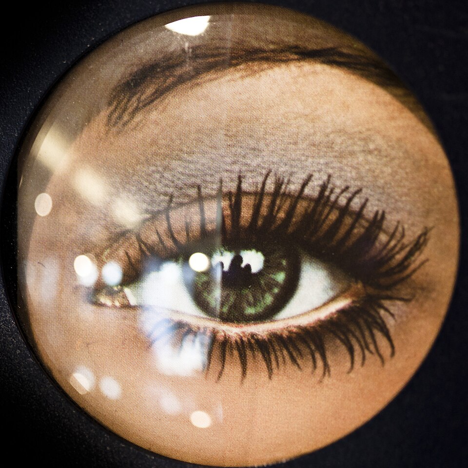
This tutorial is for readers making their first thin-film design. You will calculate the reflectance of bare glass, reduce the 550 nm reflection with one MgF₂ layer, and then extend the low-reflectance region to 450–650 nm by optimizing the thicknesses of a four-layer coating.
Calculate the Reflection from Bare Glass
Glass reflects even without a coating because air and glass have different refractive indices. At normal incidence from air, the reflectance of the glass surface is
Here, is power reflectance, is the refractive index of air, and is the refractive index of glass. Substituting and gives
In Structure, use air as the top medium, place a 1 mm glass substrate below it, and use glass again as the bottom medium.

Mark the 1 mm glass substrate as incoherent. The task is to calculate the surface reflection of a lens, not to treat millimeter-scale glass as a coherent thin film with stable interference fringes.
In Optics, set 400–700 nm with a 1 nm step, 0° incidence, unpolarized light, and enable Reflectance and Transmittance. The same settings will be used for the single-layer coating.
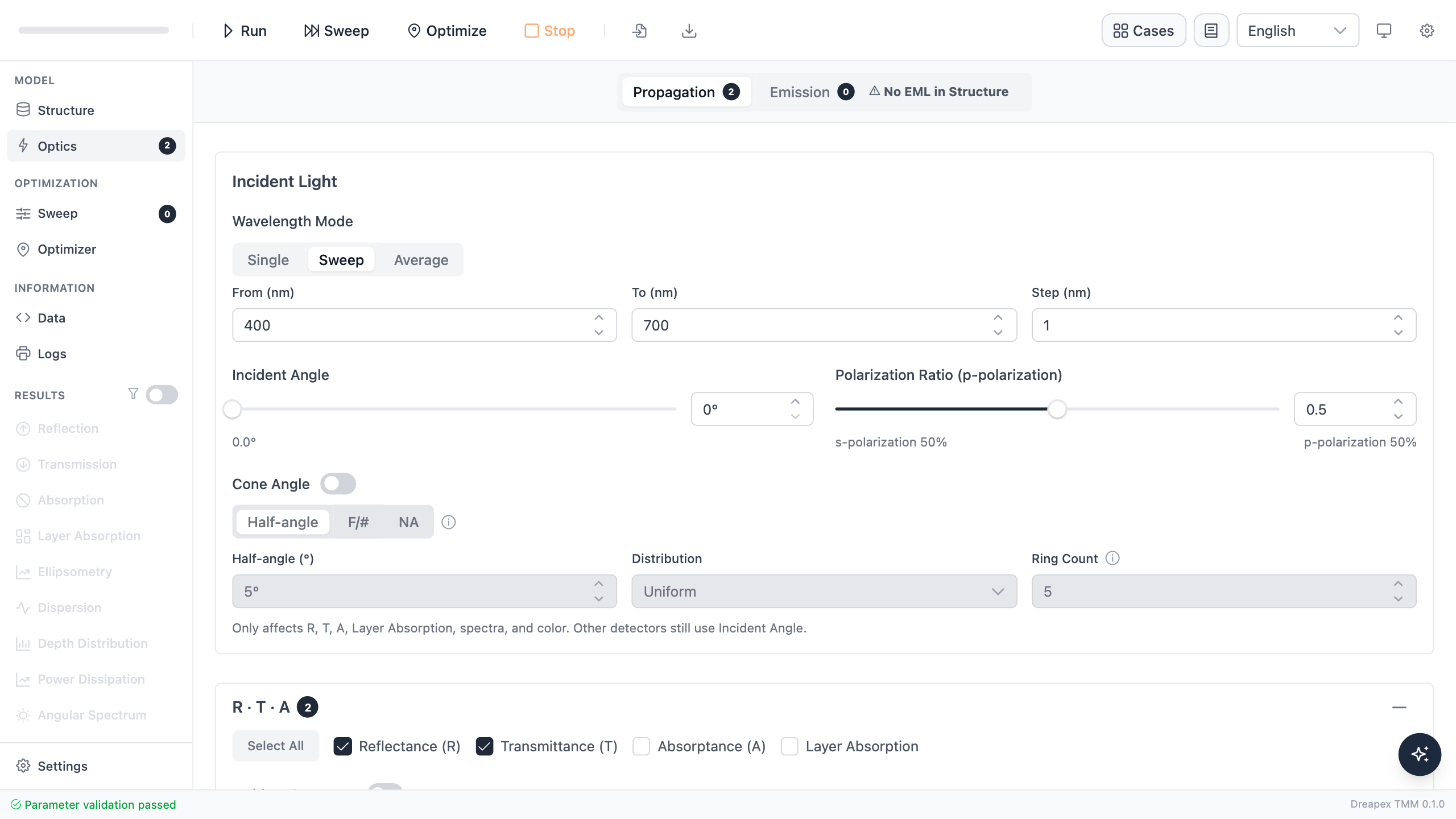
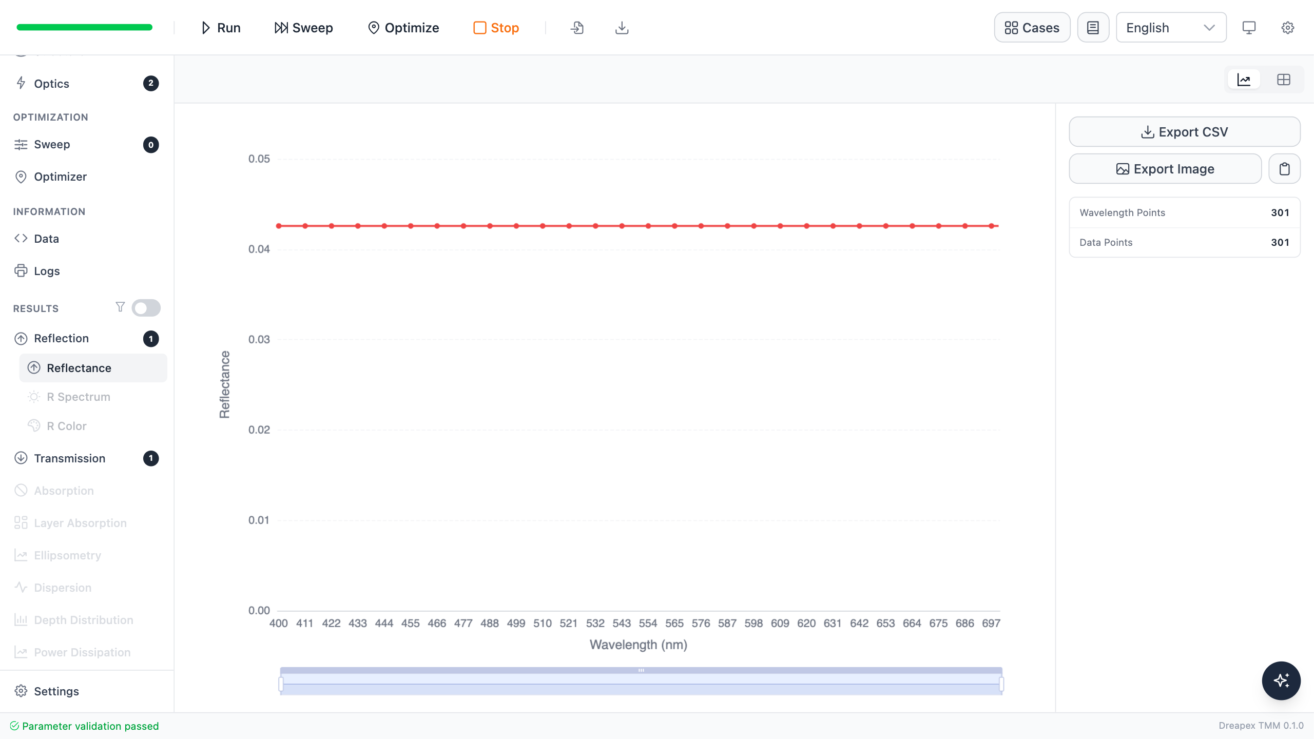
Select Run. Bare-glass reflectance remains at 4.258% across the band, while transmittance is 95.742%.
Make Two Reflected Waves Weaken Each Other
Adding a transparent film creates two main reflected waves. One returns from the air–film boundary. The other enters the film, reflects from the film–glass boundary, and then returns to air.
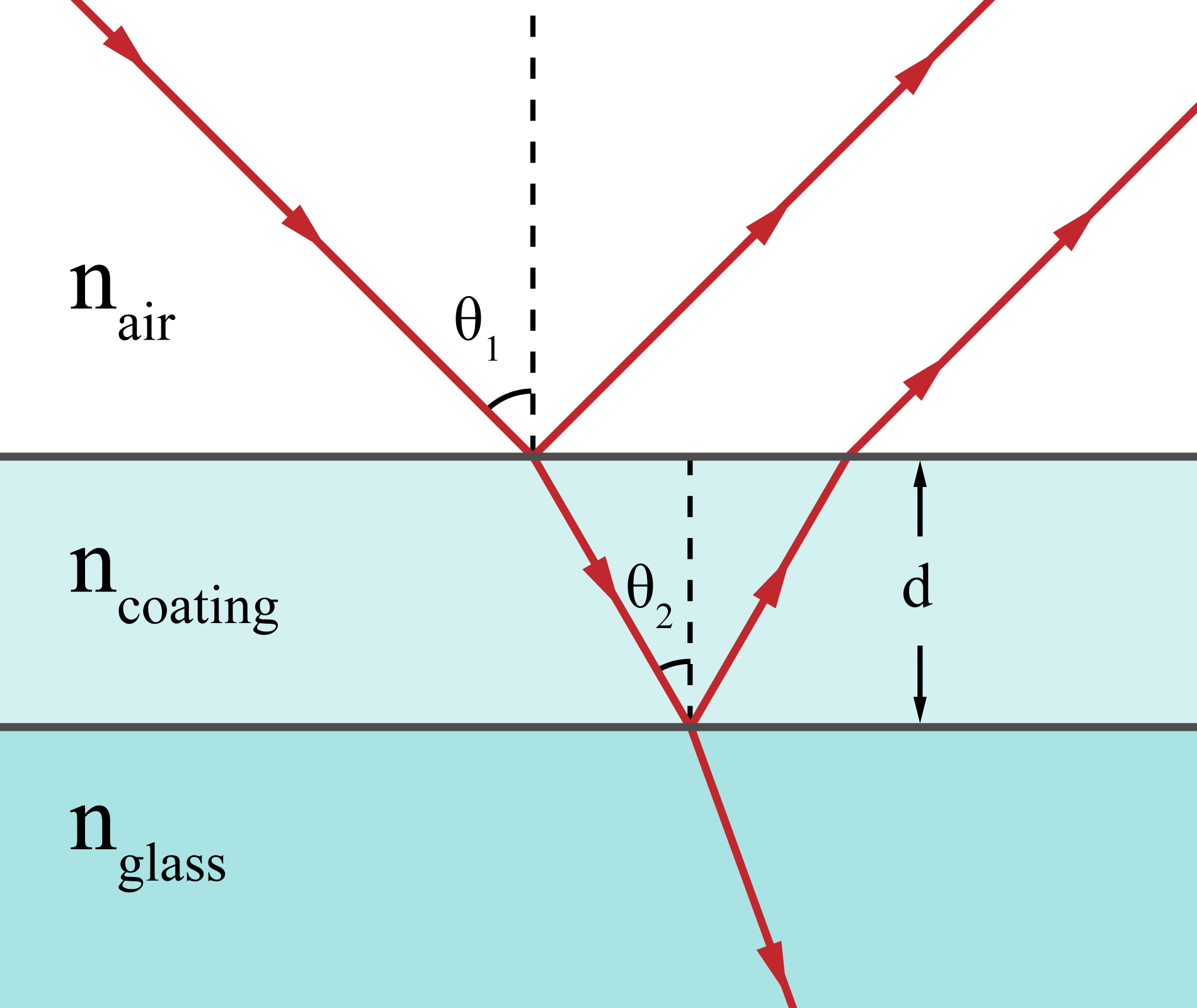
If the round-trip optical path in the film equals half the design wavelength, the second reflected wave returns half a cycle behind the first, so the two reflections weaken each other. The corresponding quarter-wave thickness is
Here, is the physical film thickness, is the vacuum design wavelength, and is the film refractive index. For MgF₂ with and ,
Add 99.64 nm of MgF₂ above the glass substrate and keep the other settings unchanged.

Select Run again. The spectrum forms a minimum near 550 nm, where reflectance falls from 4.258% for bare glass to 1.260%.
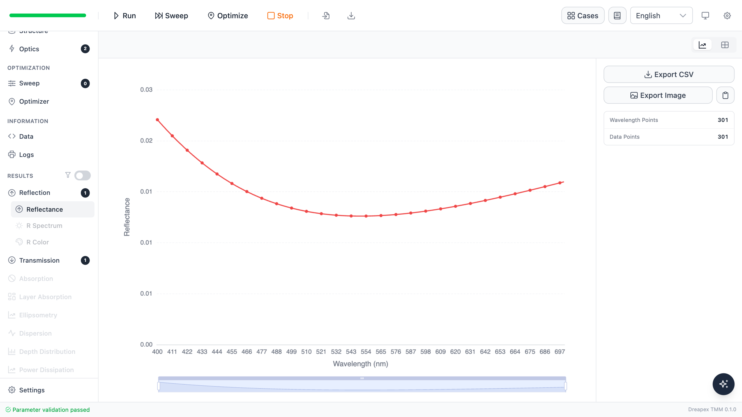
| Design | Reflectance at 550 nm |
|---|---|
| Bare glass | 4.258% |
| 99.64 nm MgF₂ on glass | 1.260% |
Why does it not reach zero? The quarter-wave thickness sets the phase relationship, but complete cancellation also requires equal reflected-wave amplitudes. The ideal index of a single AR layer is
MgF₂ has an index of 1.38 rather than 1.233. It therefore reduces the 550 nm reflection substantially but cannot produce exact zero reflectance.
Extend Low Reflectance across a Band
A single layer controls the phase around 550 nm. Camera lenses, display cover glass, and photovoltaic glass usually need low reflection over a visible band, so the next design uses four MgF₂/TiO₂ layers and expands the target to 450–650 nm.
For transparent hand-calculation examples, this tutorial uses constant indices: air 1.00, glass 1.52, MgF₂ 1.38, and TiO₂ 2.45. A production coating requires wavelength-dependent n and k data for the deposition materials.
From the air side toward the glass, the initial stack is:
| Film | Material | Initial thickness |
|---|---|---|
| 1 | MgF₂ | 99.64 nm |
| 2 | TiO₂ | 112.24 nm |
| 3 | MgF₂ | 24.91 nm |
| 4 | TiO₂ | 14.03 nm |
| Substrate | Glass | 1 mm, incoherent |
In Optics, set 400–700 nm with a 1 nm step, 0° incidence, unpolarized light, and enable Reflectance and Transmittance. The calculation range is wider than the target band so that you can see behavior both inside 450–650 nm and at its edges.
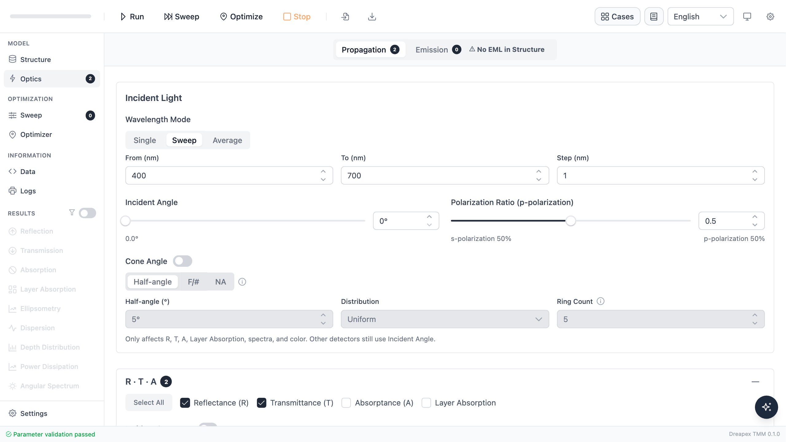
Before selecting Run, make a prediction: the initial four-layer stack should have lower band-average reflectance than the single MgF₂ layer, but its spectrum should still have ripple. The calculated four-layer baseline is 0.341% at 550 nm and 0.648% on average over 450–650 nm.
| Design | Reflectance at 550 nm | Average reflectance, 450–650 nm |
|---|---|---|
| Single MgF₂ layer | 1.260% | 1.348% |
| Initial four-layer stack | 0.341% | 0.648% |
The four layers improve the full band, but the design has not yet reached the target of less than 0.1% average reflectance.
Let the Optimizer Try the Thicknesses
Four films give four adjustable thicknesses, so manual trial and error quickly becomes inefficient. Optimizer changes those thicknesses repeatedly within limits that you provide, recalculates the spectrum, and scores each combination by its 450–650 nm average reflectance. It does not choose the materials or add layers for you; you still define the structure, target, and adjustable parameters.
In Optimizer, add one objective: minimize average Reflectance from 450 to 650 nm with a 5 nm step, at 0° with unpolarized light. Then add all four film thicknesses as variables:
| Film | Initial thickness | Range the optimizer may try |
|---|---|---|
| MgF₂ 1 | 99.64 nm | 85–115 nm |
| TiO₂ 1 | 112.24 nm | 95–135 nm |
| MgF₂ 2 | 24.91 nm | 15–40 nm |
| TiO₂ 2 | 14.03 nm | 5–25 nm |
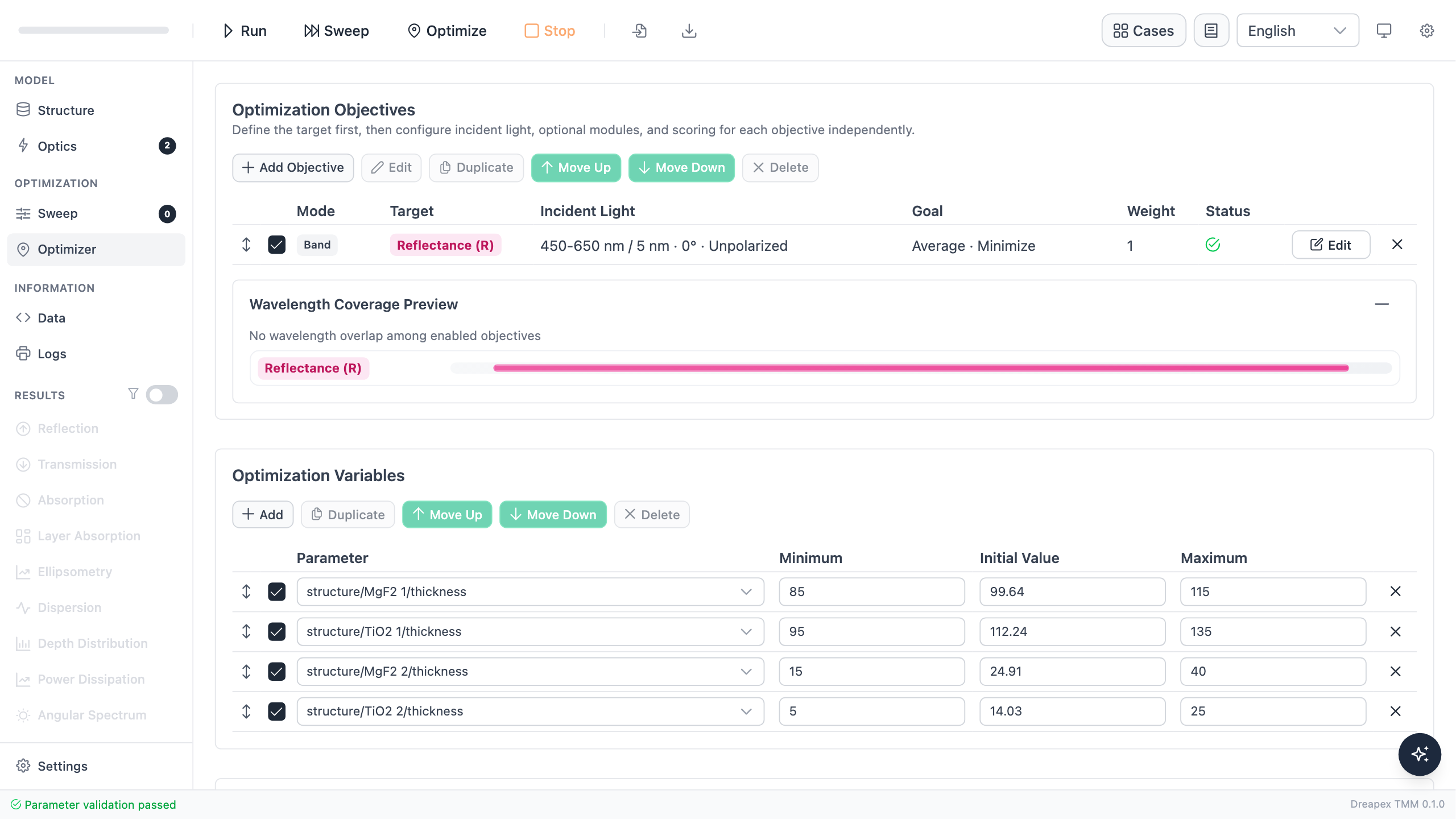
Select Nelder–Mead, set the maximum number of evaluations to 400, and set the initial simplex ratio to 0.08. Nelder–Mead compares objective values without calculating derivatives, which makes it suitable for this introductory problem with four continuous variables.
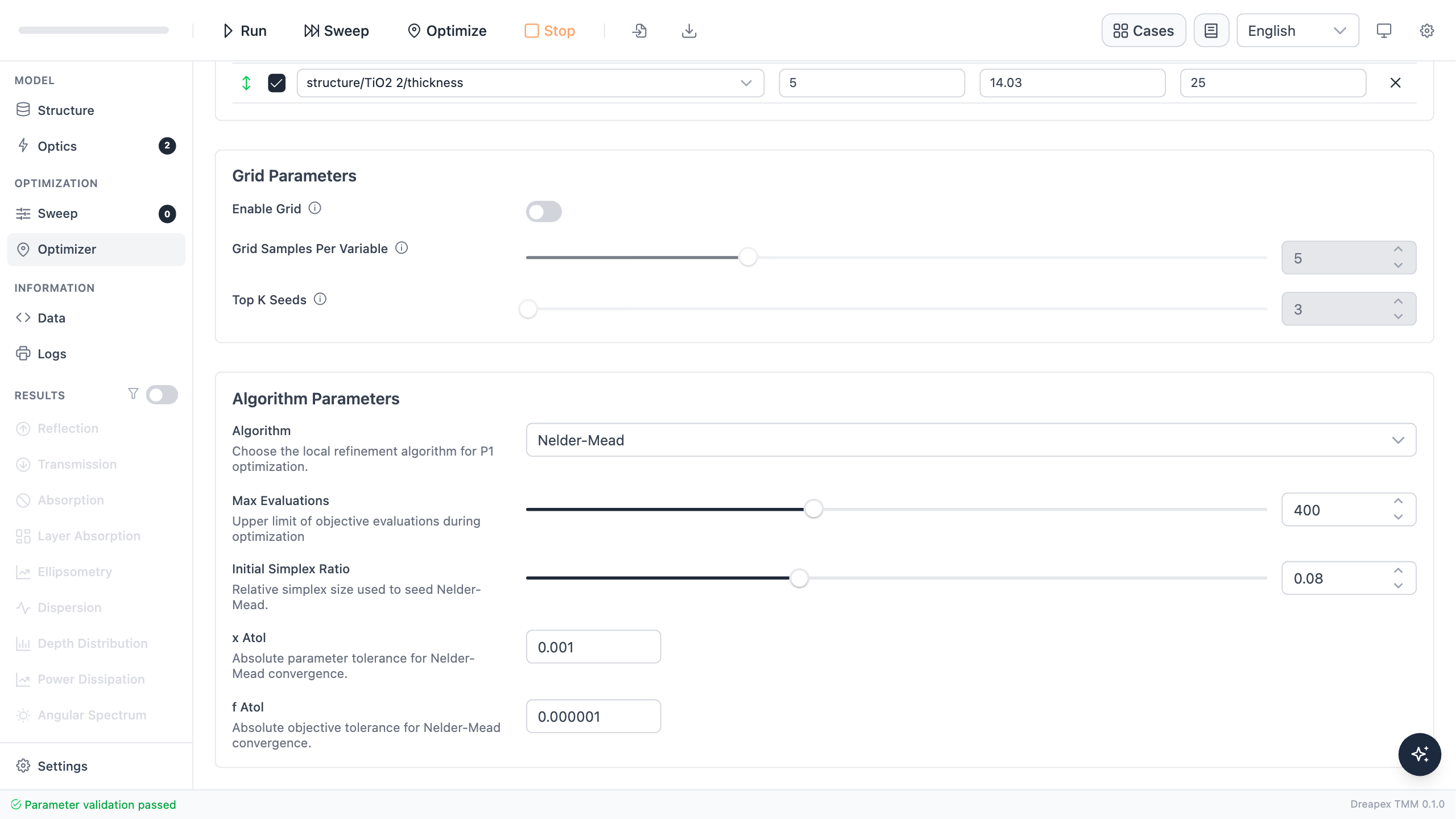
Select Optimize. This run reached the following result after 174 objective evaluations and 101 iterations. The optimized values appear only now, after the optimization has been set up and run:
| Film | Initial thickness | Optimized thickness |
|---|---|---|
| MgF₂ 1 | 99.64 nm | 97.373 nm |
| TiO₂ 1 | 112.24 nm | 116.149 nm |
| MgF₂ 2 | 24.91 nm | 37.769 nm |
| TiO₂ 2 | 14.03 nm | 11.108 nm |
Select Apply to Structure, return to Structure, and confirm that all four values were written back. Then run a forward calculation with a finer 1 nm step. Optimization uses 5 nm sampling to reduce the calculation cost, while final validation uses 1 nm sampling, so the two pages may report slightly different averages.

Optimized Result Against the Target
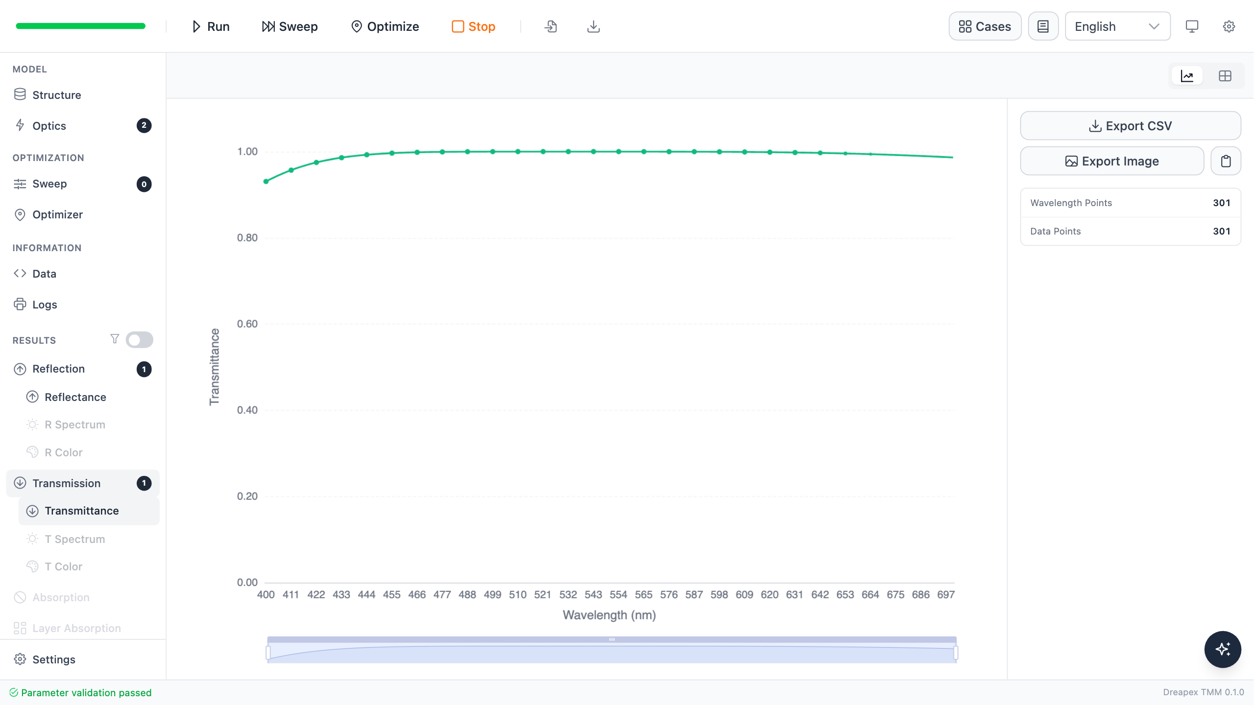
The optimized average reflectance over 450–650 nm is 0.0865%, which passes the 0.1% target. Reflectance is 0.00110% at 550 nm. The maximum within the band is 0.5005% at 450 nm.
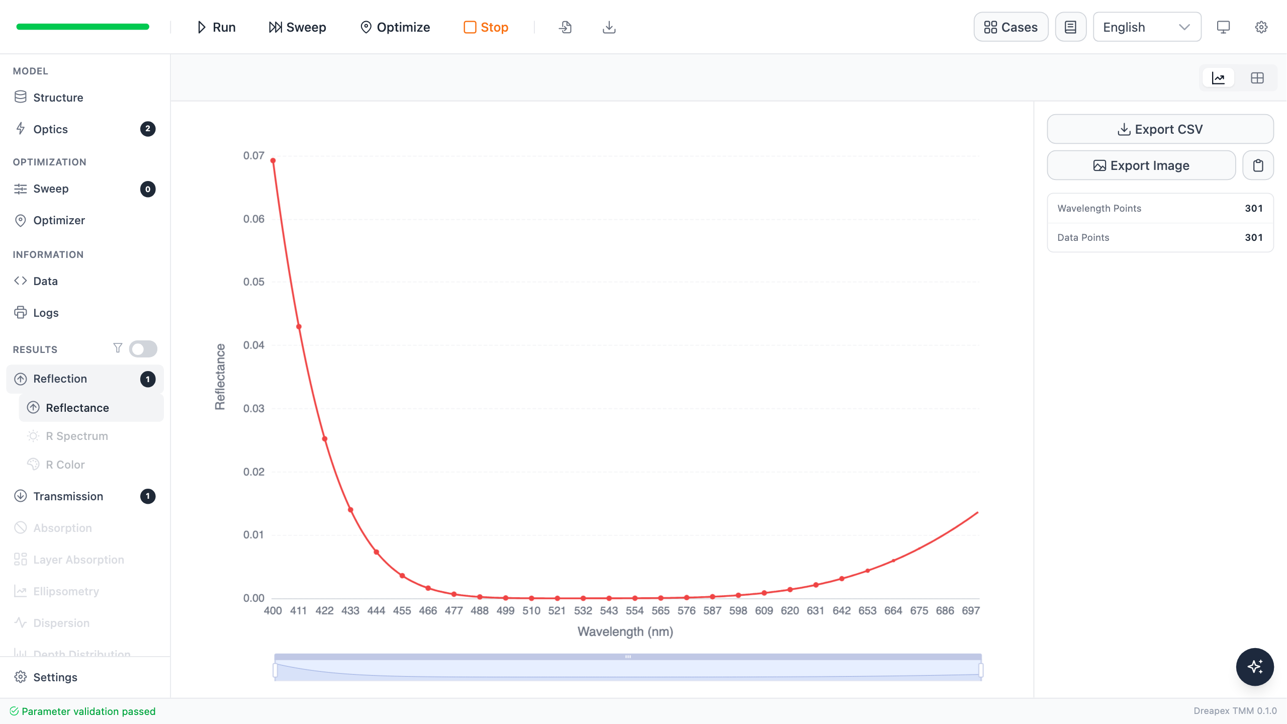
Reflectance rises to 6.924% at 400 nm. This is not a failed calculation: the objective constrains only 450–650 nm, and the optimizer does not automatically improve wavelengths outside that range.
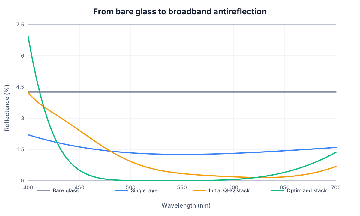
| Design | Reflectance at 550 nm | Average reflectance, 450–650 nm |
|---|---|---|
| Bare glass | 4.258% | 4.258% |
| Single MgF₂ layer | 1.260% | 1.348% |
| Initial four-layer stack | 0.341% | 0.648% |
| Optimized four-layer stack | 0.00110% | 0.0865% |
Every material in this teaching model is lossless, so the result should satisfy . Energy removed from reflection becomes transmitted light; it does not disappear.
Change One Thickness Yourself
Restore the four-layer stack to its initial thicknesses, then change only the first MgF₂ layer to 90, 99.64, and 110 nm. Before each run, predict whether the reflectance minimum will move toward shorter or longer wavelengths. Then compare the 550 nm reflectance and the 450–650 nm average. This experiment shows directly that the best thickness for one wavelength is not necessarily the best thickness for a full band.
For an engineering design, replace the constant indices with wavelength-dependent n and k data for the deposition process, then repeat the checks for angle, polarization, and thickness error.
← Back to Tutorial Catalog · Next: A Mirror Made of Transparent Materials