Anisotropic OLED outcoupling
Simulation method for study on outcoupling characteristics of stratified anisotropic OLEDs
Authors: Xianhua Ke, Honggang Gu, Xuenan Zhao, Xiuguo Chen, Yating Shi, Chuanwei Zhang, Hao Jiang, and Shiyuan Liu
Journal: Optics Express 27(16), A1014–A1029 (2019) · Comparison target: Figure 3
An organic light-emitting diode (OLED) emitting through a glass substrate contains a transparent anode, organic transport layers, an emission layer, and a metal cathode. The distance between the emission layer and metal controls cavity interference; dipole orientation and transport-layer birefringence further change outcoupling and the far-field angular distribution. Ke et al. study these relationships using an Alq3 emission layer, a TPD hole transport layer (HTL), and a BCP electron transport layer (ETL).
This case compares the thickness response in Figure 3 at 539 nm. It shows only comparisons with identifiable inputs that agree with the paper.
Structure
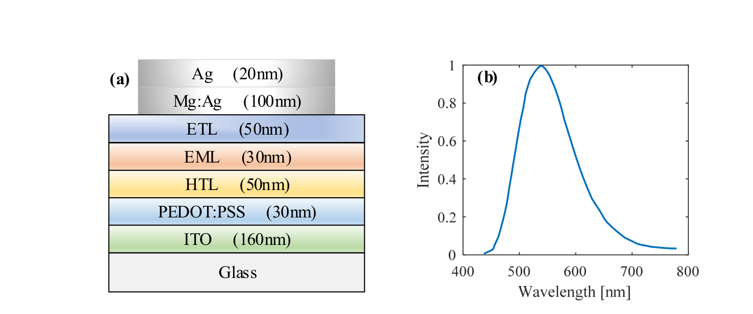
Light exits through the glass side. In Structure, enter the following layers downward from the air Top Medium, with glass first and the metals last. Set Bottom Medium to air as well, with refractive index 1. Set each layer name and thickness, enable Emis. for EML / Alq3, and enable Inco. for Glass substrate. Enable Tran. for both glass and the emission layer.
| Layer | Thickness | Layer status |
|---|---|---|
| Glass substrate | 1 mm | Inco. / Tran. |
| ITO | 160 nm | None |
| PEDOT:PSS | 30 nm | None |
| HTL / TPD | 50 nm | None |
| EML / Alq3 | 30 nm | Emis. / Tran. |
| ETL / BCP | 50 nm | None |
| Mg:Ag (60:1) | 100 nm | None |
| Ag | 20 nm | None |
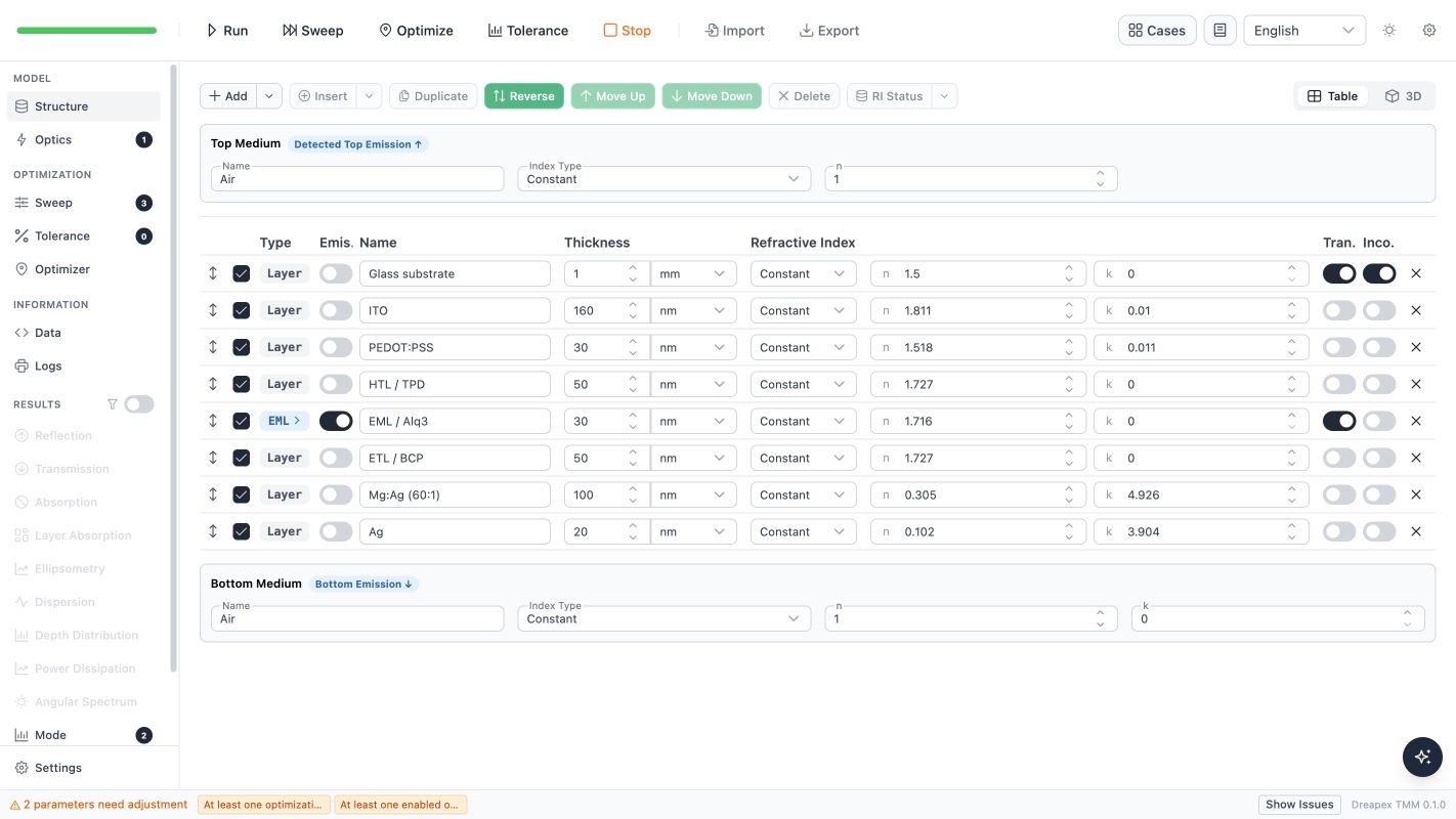
Initially set each Index Type to Constant. Here is the real refractive index and the extinction coefficient; both are dimensionless. Values for the seven internal layers come from Table 1 and apply only at 539 nm. The glass index and thickness are assumptions in this reconstruction, not measured inputs supplied by the paper.
| Layer | Source | ||
|---|---|---|---|
| Glass substrate | 1.500 | 0 | Incoherent-glass assumption |
| ITO | 1.811 | 0.010 | Table 1 |
| PEDOT:PSS | 1.518 | 0.011 | Table 1 |
| HTL / TPD | 1.727 | 0.0000319 | Table 1 |
| EML / Alq3 | 1.716 | 0 | Table 1; transparent emission layer |
| ETL / BCP | 1.727 | 0.0000319 | Table 1 |
| Mg:Ag (60:1) | 0.305 | 4.926 | Table 1 |
| Ag | 0.102 | 3.904 | Table 1 |
Emission-spectrum input
Download the 539 nm monochromatic input. It contains wavelength 539 nm and unit weight 1, prepared for this monochromatic calculation. It does not replace the full photoluminescence spectrum in Figure 2(b).
Emitter settings and thickness sweep
A horizontal electric dipole (HED) lies parallel to the layer plane; a vertical electric dipole (VED) lies along its normal. Open the emitter editor for EML / Alq3, name the emitter 539 nm emitter, and apply the settings below. In Custom, is the vertical orientation fraction: gives HED and gives VED. Mixed orientations are not swept here.
| Field | Setting |
|---|---|
Spectrum Type | File; upload the monochromatic input |
Spectrum Unit | Probability |
Dipole Orientation | Custom, initially |
Position (0-1) | 0.5, the emission-layer center |
Distribution | Delta |
Quantum Efficiency (0-1) | 1 |
Lifetime | 1 ns |
Conversion Efficiency (0-1), Multiplication Factor | Both 1 |

In Optics, enable only Mode, set Wavelength Mode to Single, and set Wavelength to 539 nm.

In Sweep, use Add to create the ETL-thickness and orientation items below. Keep quantum efficiency at 1 and run the 400 combinations for Figure 3 first.
Parameter | From | To | Sampling | Step |
|---|---|---|---|---|
ETL / BCP → thickness | 2 | 400 | Step | 2 nm |
539 nm emitter → dipoleOrientationValue | 0 | 1 | Step | 1 |
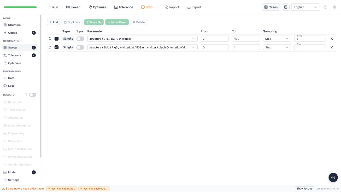
Click the toolbar Sweep and wait for completion. The notices about missing optimization objectives and variables do not block this sweep. Download the 400 Dreapex TMM mode-sweep records for Figure 3 to inspect the curves shown here.
Thickness-dependent outcoupling and decay (Figure 3)
After running, open Mode → Distribution, selecting Line and Top Outcoupling; open Mode → Emission, selecting Line and Decay Rate Enhancement. Legend values 0.000 and 1.000 mean HED and VED. Outcoupling is a fraction; multiply by 100 for percent.
At quantum efficiency , the first HED outcoupling maximum is 34.30% at an ETL thickness of 30 nm. VED reaches 10.17% at 138 nm. The two orientations have different peak positions, and the HED outcoupling maximum does not coincide with its decay-rate maximum.
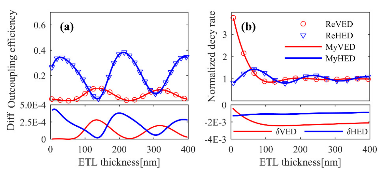
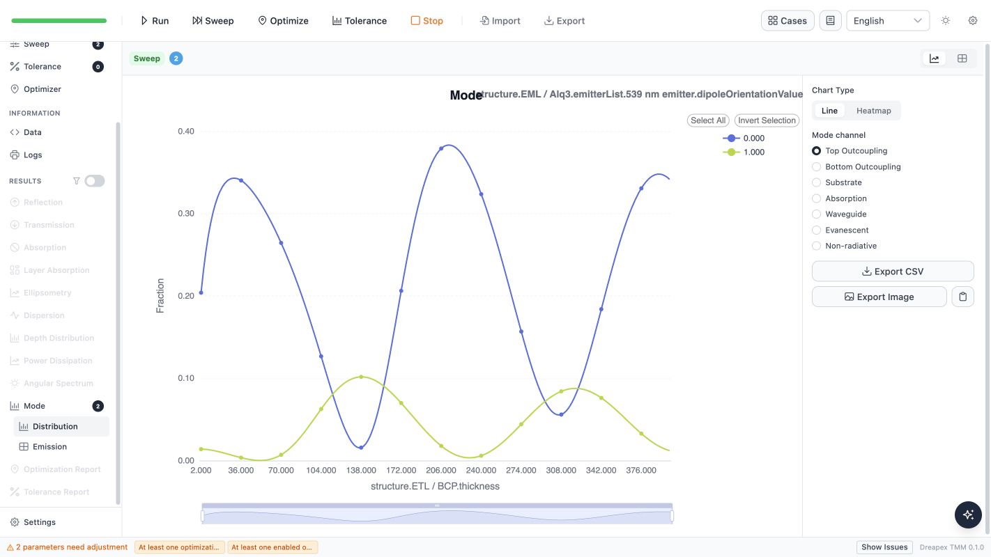
Software result: Figure 3 outcoupling; legend 0 is HED and 1 is VED
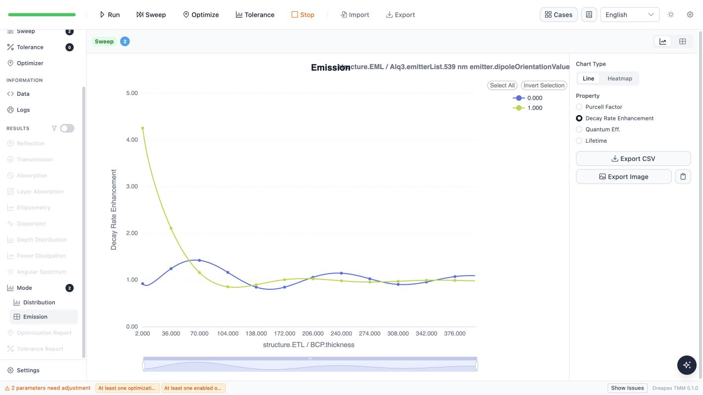
Software result: Figure 3 normalized decay rate
The upper curves of Figure 3 were extracted from pixels and compared at matching thicknesses from 10 to 390 nm. Root-mean-square differences in outcoupling are approximately 0.32 percentage points for VED and 0.45 for HED; normalized-decay-rate differences are approximately 0.019 and 0.015. These differences correspond to about 1.1–2.0 vertical pixels in the paper PNG, comparable to the uncertainty introduced by line width and hollow markers. The paper reports rounded 539 nm optical constants and does not specify the glass index or outer boundary, so the remaining difference cannot be assigned uniquely to one input parameter.
The lower panels of Figure 3 show the paper's method minus the Celebi method, not Dreapex TMM errors, the software screenshots compare only the two physical quantities in the upper panels. The software decay-rate axis extends to 5 to show the complete VED result at 2 nm ETL thickness.
Paper figures not included
- Figures 4 and 5: The full emission spectrum and material dispersion are unavailable.
- Figures 6 and 7: Their curves are inconsistent with Figure 3, and scanning the emitter position did not produce a common input.
- Figures 8 and 9: The fixed ETL thickness and angle convention are unspecified; thickness, emitter-position, and glass-internal-angle scans found no common input that matches both VED and HED.
- Figure 10: The paper accumulates power by physical region—Air, Glass, ITO, Organic, and Top contact—whereas software
Modegroups power by in-plane-wavevector ranges such as outcoupling, substrate guiding, device guiding, and evanescent coupling. Four air-outcoupling endpoints can be checked, but the complete stacks do not represent the same quantities.
Comparison scope
This case compares only the thickness-dependent outcoupling and decay curves in Figure 3. Other paper figures are excluded because of missing inputs, inconsistent cross-figure conditions, or different output-group definitions.