OLED Waveguide-Mode Suppression with an Ultrathin Metal Anode
Tackling light trapping in organic light-emitting diodes by complete elimination of waveguide modes
Authors: Changyeong Jeong, Yong-Bum Park, and L. Jay Guo
Journal: Science Advances 7, eabg0355 (2021) · Comparison target: Figure 1 and Table 1 · License: CC BY-NC 4.0
The paper's 140 nm organic stack is thicker than the ITO device's 69 nm first-order transverse-magnetic mode (TM₁) cutoff, while it is thinner than the 208 nm fundamental transverse-electric mode (TE₀) and 236 nm TM₁ cutoffs of the 5 nm Cu-seeded Ag electrode. The reported Waveguide fraction consequently falls from 16.0% to 0%. This case tests that mode-transfer mechanism in Dreapex TMM at the 530 nm emission peak, using open optical constants and a disclosed effective electrode proxy. The Figure 1 cutoff consequence is the primary target; Table 1 is a semi-quantitative point of comparison because the paper integrates that table over the emission spectrum.
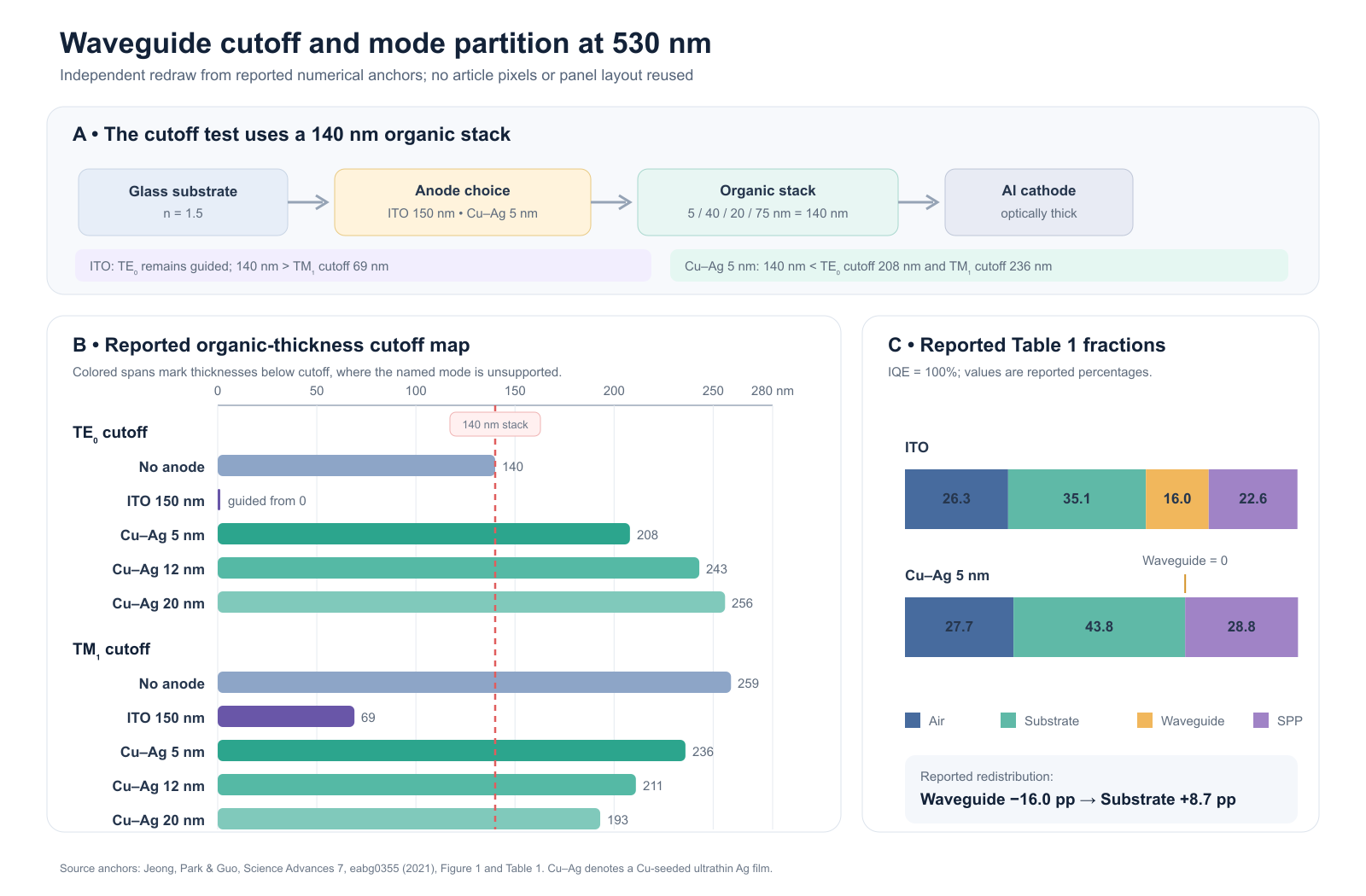
The red 140 nm marker falls in the unsupported region for both Cu-seeded Ag cutoffs. The same thickness remains above the ITO TM₁ cutoff, and the paper reports that the ITO TE₀ mode is guided even as organic thickness approaches zero.
Background
A planar OLED guides light when its organic and electrode stack can sustain an in-plane optical mode. A cutoff thickness marks the boundary below which a named mode is no longer supported. Jeong et al. identify two relevant branches at 530 nm: a dielectric-like TE₀ mode and a metal-sensitive TM₁ mode.
The ultrathin electrode changes the two branches through different physical levers. Its negative real permittivity weakens TE₀ confinement, while replacing 150 nm ITO with only 5 nm of metal reduces the total guiding thickness seen by TM₁. The practical consequence is the same for the paper's 5/40/20/75 nm organic stack: both branches are below cutoff with the ultrathin electrode.
The Mode result performs a complete power budget after an emitting dipole couples into the planar stack. Power Dissipation retains the in-plane-wave-vector view and can show whether a guided peak survives. These are emission calculations; externally incident reflectance or transmittance alone cannot establish the OLED mode budget.
Mapping the Paper to the TMM Model
The paper's Figure 2 optical model replaces the simplified CBP slab of Figure 1 with an archetypal multilayer OLED. The organic total remains 140 nm, so the Figure 1 cutoff comparison directly predicts the presence or absence of its waveguide channel.
Structure from the output side to Al
In the table, denotes power reflectance and denotes power transmittance; both are dimensionless fractions reported as percentages.
| Layer | Thickness | Optical constant at 530 nm | Source and modeling status |
|---|---|---|---|
| Glass, incoherent | 1 mm | 1.5000 | Paper assumption |
| ITO reference | 150 nm | 1.8833 + 0.00343i | Open ITO dataset near 530 nm |
| Cu-seeded Ag alternative | 5 nm | 0.283728 + 3.712435i | Effective-film proxy independently inferred from the paper's calculated bare-film R = 15.2% and T = 78.4% at 550 nm |
| MoO₃ | 5 nm | 1.86114 + 0.00487i | Open MoO₃ dataset near 530 nm |
| TAPC | 40 nm | 1.678484 | Aulika et al. open OLED optical data |
| 10% Ir(ppy)₂acac in CBP, emissive | 20 nm | 1.828176 | CBP sample from Aulika et al. open OLED optical data |
| TPBi | 75 nm | 1.763003 | Aulika et al. open OLED optical data |
| Al | 150 nm | 0.9303 + 6.3964i | Open Al data interpolated to 530 nm |
The Cu-seeded Ag film is approximately 5 nm Ag grown on a Cu seed, not a bulk Cu–Ag alloy. The effective value above reproduces the publicly reported and of the complete ultrathin film on glass to the reported precision. It is not the authors' original ellipsometry and is held constant from 550 to 530 nm for this single-wavelength test.
Emission and detector settings
The normalized in-plane wave vector is , where is the magnitude of the wave-vector component parallel to the layers, is the vacuum wave number, is the emissive-layer refractive index at that wavelength, is the emissive-layer wave number, and is the vacuum wavelength. The wave numbers have inverse-length units, so is dimensionless.
| Setting | Value |
|---|---|
| Emitter | Ir(ppy)₂acac in the center of the 20 nm EML |
| Dipole distribution | Delta, relative position 0.5 |
| Dipole orientation | Custom, vertical-dipole fraction 0.23, corresponding to the reported orientation factor 0.77 |
| Intrinsic radiative quantum efficiency | 1.0, matching the ideal optical calculation |
| Spectrum | Unit White; no broadband weighting in a single-wavelength calculation |
| Detectors | Mode and Power Dissipation |
| Wavelength | Single, 530 nm |
| Power-dissipation coordinate | , 0–2, step 0.002 |
Mode-channel mapping
Surface plasmon polariton (SPP) denotes a bound electromagnetic mode at a metal–dielectric interface. The paper uses this label for the high-in-plane-wave-vector power beyond the EML wave number.
| Paper channel | Dreapex TMM channel | Comparison status |
|---|---|---|
| Air | Top Outcoupling | Direct |
| Subs | Substrate | Direct |
| W/G | Waveguide | Direct and primary acceptance channel |
| SPP | Evanescent | Both cover the region above the EML wave number; Absorption remains separate |
| Not separated by the paper | Bottom Outcoupling | Reported separately |
| Not separated by the paper | Non-radiative | Reported separately; expected to approach zero for intrinsic radiative quantum efficiency 1 |
The paper places all power above the EML wave number into SPP, and Dreapex TMM uses the same interval for Evanescent. Absorption is residual power below the EML light line that does not enter an escape channel, so it remains separate and cannot be added to SPP.
Reproduction Target and Acceptance Criteria
The following criteria were defined before the results were compared:
- Both models must complete the
ModeandPower Dissipationcalculations. - Each seven-channel
Modebudget must close to100%within0.01percentage point. - The Cu-seeded Ag model must return at most
2.0%Waveguide power and at least10.0percentage points less Waveguide power than ITO. - The Cu-seeded Ag Substrate fraction must exceed the ITO Substrate fraction.
- Top Outcoupling and Substrate must each be within
10.0percentage points of their Table 1 anchors for both models. - ITO Waveguide must be within
10.0percentage points of16.0%; Cu-seeded Ag Waveguide uses the stricter2.0%ceiling. - SPP is compared directly with Evanescent, while Absorption is reported independently. SPP is not the sole first-pass criterion because this case uses one
530 nmpoint whereas Table 1 is spectrum-integrated.
A missed criterion remains a reported failure. Material constants, thicknesses, dipole settings, and thresholds are not tuned after seeing the result; any alternative is labeled as a separate sensitivity run.
Modeling Path in Dreapex TMM
Structure
Import the two benchmark inputs:
The layer sequence runs from the incoherent Glass output side to the optically thick Al cathode. The two inputs differ only in the anode layer. The EML remains emissive in both.
Optical Settings
In the Emission detector lane, keep Mode and Power Dissipation enabled. Set both wavelength controls to Single at 530 nm; set the Power Dissipation coordinate from 0 to 2 with a 0.002 step. Run each imported model once.
Example Setup
The table below is the compact reconstruction checklist for both inputs. The anode row is the only variant.
| Item | ITO reference | Cu-seeded Ag alternative |
|---|---|---|
| Anode | 150 nm, 1.8833 + 0.00343i | 5 nm, 0.283728 + 3.712435i |
| Organic sequence | MoO₃ 5 / TAPC 40 / EML 20 / TPBi 75 nm | Same |
| Emitter | Center of EML, vertical fraction 0.23, intrinsic radiative quantum efficiency 1 | Same |
| Calculation | Mode + Power Dissipation, 530 nm | Same |





The screenshots show the settings contained in the two downloadable benchmark models.
Simulation Results and Comparison with Figure 1 and Table 1
Figure 1 supplies the cutoff mechanism, while Table 1 supplies an integrated mode budget. The primary numerical verdict uses the 530 nm Waveguide, Substrate, and Top Outcoupling channels.
Mode Budget


| Channel | Paper ITO | Simulated ITO | Paper Cu-seeded Ag | Simulated Cu-seeded Ag | Change in simulation |
|---|---|---|---|---|---|
| Air / Top Outcoupling | 26.3% | 21.80% | 27.7% | 23.15% | +1.35 pp |
| Substrate | 35.1% | 35.48% | 43.8% | 39.91% | +4.42 pp |
| Waveguide | 16.0% | 24.30% | 0% | 15.52% | −8.78 pp |
| SPP / Evanescent | 22.6% | 13.19% | 28.8% | 7.80% | −11.59 pp |
| Bottom Outcoupling | Not separated | 0.00% | Not separated | 0.00% | 0.00 pp |
| Non-radiative | Not separated | 0.00% | Not separated | 0.00% | 0.00 pp |
The single-wavelength calculation reproduces the direction of the paper's transfer from Waveguide power into Substrate and high-wave-vector channels, but not the reported complete elimination. The Waveguide reduction is 8.78 pp, leaving 15.52% rather than the paper's 0%.
In-Plane-Wave-Vector Evidence
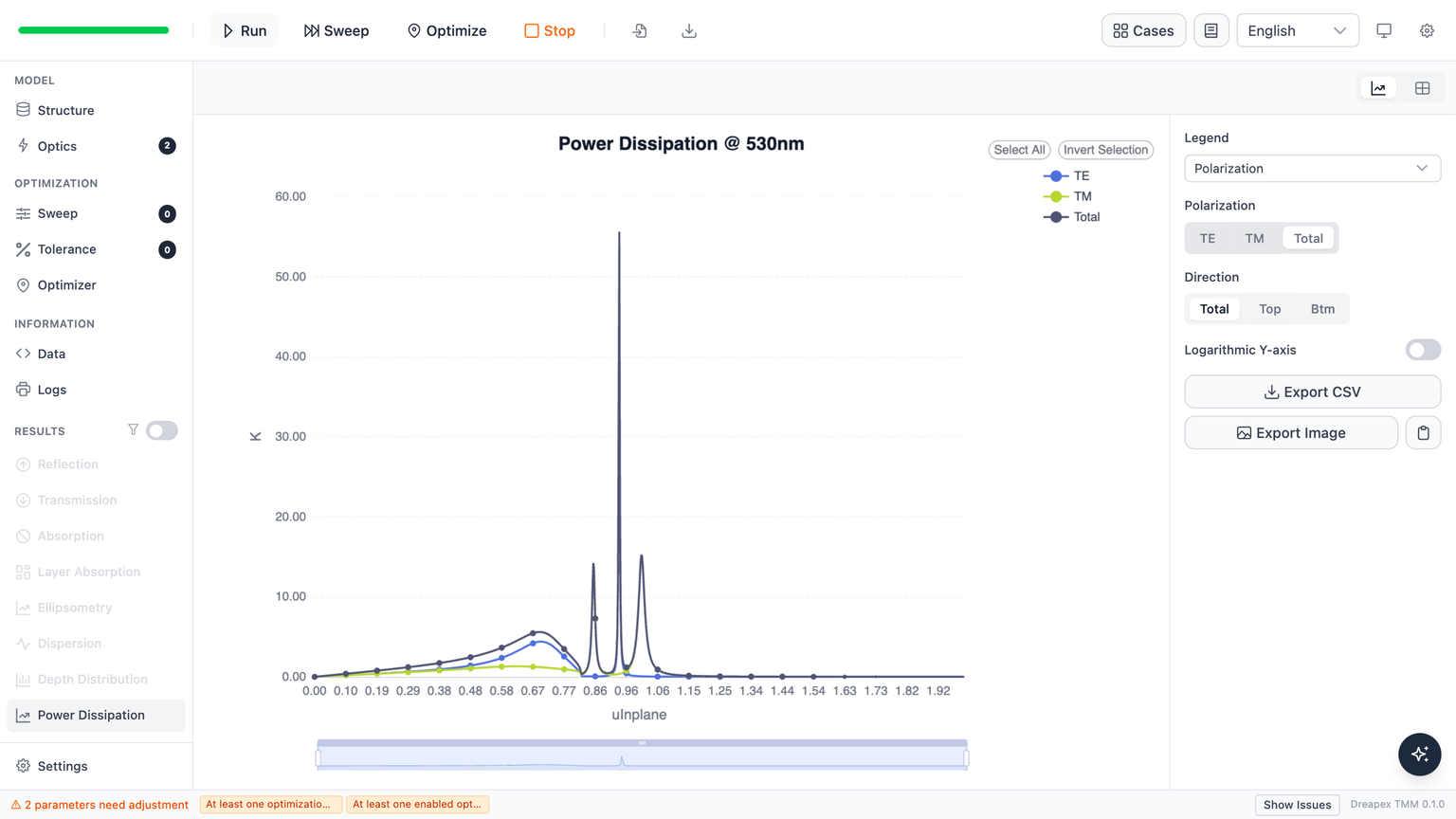
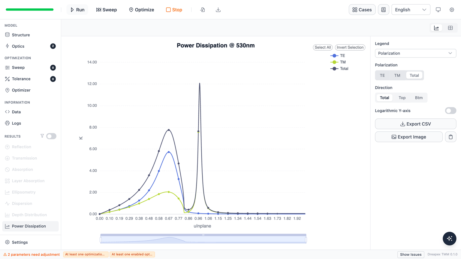
The ITO result contains several narrow peaks between approximately and . The effective ultrathin-electrode model has a TM-dominated narrow peak near ; this point remains inside the paper's Waveguide interval and cannot be dismissed as a channel-naming difference. The integrated Mode Waveguide fraction remains the numerical acceptance criterion.
Acceptance Verdict
The overall verdict is Fail: eight of ten checks pass. Both power budgets close to 100%, all four Air/Substrate values stay within 10 pp of Table 1, ITO Waveguide is within 10 pp, and the Cu-seeded Ag Substrate share exceeds ITO by 4.42 pp. The two failed checks are the ≤2% Cu-seeded Ag Waveguide ceiling and the required ≥10 pp Waveguide reduction; the calculated values are 15.52% and 8.78 pp, respectively.
Deviation Analysis
- The authors measured material permittivities by spectroscopic ellipsometry but did not publish a complete numeric table in the main article. Open single-wavelength values replace the unavailable TAPC, CBP, TPBi, ITO, MoO₃, and Al curves.
- The Cu-seeded Ag constant is an effective inversion of the reported calculated bare-film
RandT. It is neither bulk Ag nor the authors' original dispersion, and holding its550 nmvalue at530 nmis a disclosed extrapolation. The fitted real permittivity is−13.70, compared with the article's approximate visible value of about−10; the difference remains an input uncertainty rather than being tuned away. - The Figure 2 optical-stack description omits the fabricated
1.5 nmLiQ layer and3 nmAZO passivation. The primary model follows that optical description; both thin layers belong in separate sensitivity checks. - The paper's Table 1 is spectrum-integrated, whereas this primary comparison is monochromatic at the
530 nmpeak. A broad EL spectrum is unnecessary for the cutoff verdict but necessary for exact Table 1 weighting. - The paper's SPP and Dreapex TMM's Evanescent both cover the region above the EML wave number; Absorption is reported separately.
- The model is planar and one-dimensional. Roughness, scattering, electrode nonuniformity, electrical balance, exciton quenching, and substrate extraction structures are outside the optical comparison.
Further Extensions
- Sweep TPBi thickness while keeping the other layers fixed to reproduce the mode-transfer curves in Figure 2C and 2D.
- Load the measured Ir(ppy)₂acac EL spectrum and full dispersive optical constants, then repeat
Modewith spectrum weighting for a stricter Table 1 comparison. - Add
3 nmAZO and1.5 nmLiQ as separately named sensitivity variants; do not replace the primary benchmark inputs. - Vary the effective electrode constant within the uncertainty allowed by the public
R/Tanchors and report the resulting Waveguide ceiling. - Compare the ITO and ultrathin-electrode Power Dissipation peaks across
100–260 nmtotal organic thickness to connect the integrated budget to the reported cutoff map.
References
- C. Jeong, Y.-B. Park, and L. J. Guo, “Tackling light trapping in organic light-emitting diodes by complete elimination of waveguide modes,” Science Advances 7, eabg0355 (2021). DOI
- Aulika et al., open optical constants for OLED materials, CC BY 4.0. Zenodo dataset
- M. N. Polyanskiy, refractiveindex.info database. Open database repository