Audit of a Near-Infrared Tandem OLED Microcavity Simulation
Cell proliferation effect of deep-penetrating microcavity tandem NIR OLEDs with therapeutic trend analysis
Authors: Yongjin Park, Hye-Ryung Choi, Yongmin Jeon, Hyuncheol Kim, Jung Won Shin, Chang-Hun Huh, Kyoung-Chan Park, and Kyung-Cheol Choi
Journal: Scientific Reports 12, 10935 (2022) · Licence: CC BY 4.0
Park et al. used two tandem emission units in an Ag/Al metal microcavity to set the target peak of a near-infrared organic light-emitting diode (OLED) between 710 and 770 nm. This page compares Figures 1c, 3, 4f, S4, S6, S8, and S16 one by one. Every software image is a real Dreapex TMM result-page screenshot captured after Run or Sweep; its visible caption identifies the paper panel, quantity, and coordinate conversion that it addresses.
“Correspondence” here means that the independent variable, dependent variable, and chart type match. It does not imply numerical reproduction. The non-cavity spectra and the peak of single-unit device A are close to the paper. The tandem microcavity recovers the two diagonal mode families and their red-shift direction, while the absolute cavity positions and complete tandem-device spectra do not close quantitatively. The paper states that the complex refractive indices of all organic layers were measured by ellipsometry but does not publish those data, so the current models use public material data and the proxies listed below.
| Paper figure | Published chart | Software evidence | Correspondence |
|---|---|---|---|
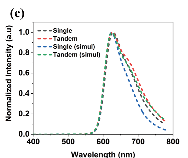
| Figure 1c | Measured and simulated single/tandem normalized spectra overlaid on one axis | Two Normalized Spectrum result pages | Split correspondence. The quantity and wavelength range match, but the software screenshots do not overlay two separate models |
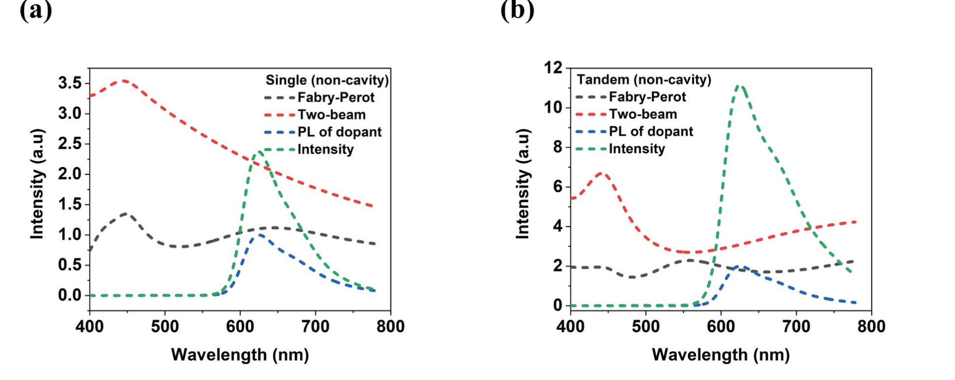
| Figure S4 | PL, Fabry–Pérot factor, two-beam factor, and final intensity | Two Intensity result pages | Partial correspondence. The screenshots cover only the final Intensity, not the first three decomposed quantities |
| Figures 3a–d | Narrow-range 2D intensity maps at 710, 730, 750, and 770 nm | Four separate narrow-range Heatmap screenshots | Direct chart-type correspondence. Each paper panel is followed by the software result at the same wavelength; coordinates use the conversion below |
| Figures S6a–d | Wide-range 2D intensity maps at the same four wavelengths | Four separate wide-range Heatmap screenshots | Direct chart-type correspondence. The UI axes are per-unit thicknesses; the paper axes are totals for both units |
| Figure S8 | Four intensity curves for 15, 20, 30, and 40 nm Ag | One Intensity page with exactly those four curves visible | Direct chart-type correspondence. The curve set matches, while lineshapes and linewidths do not |
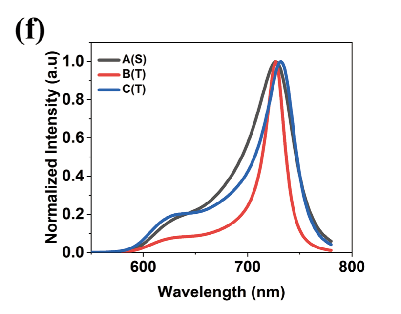
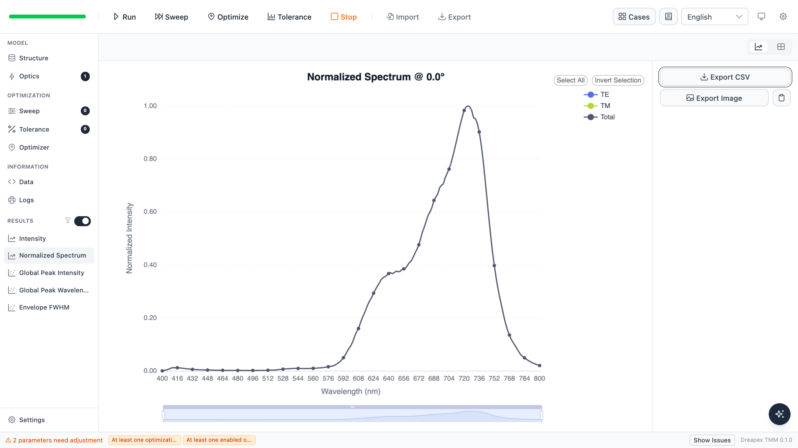
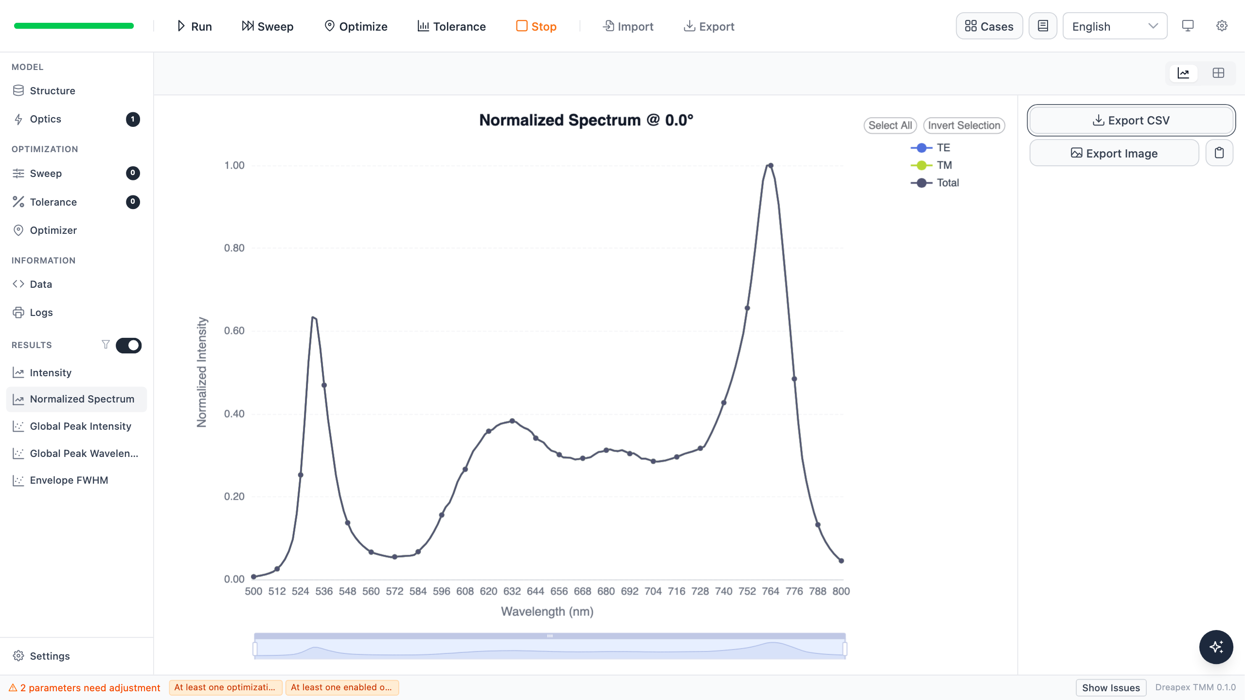
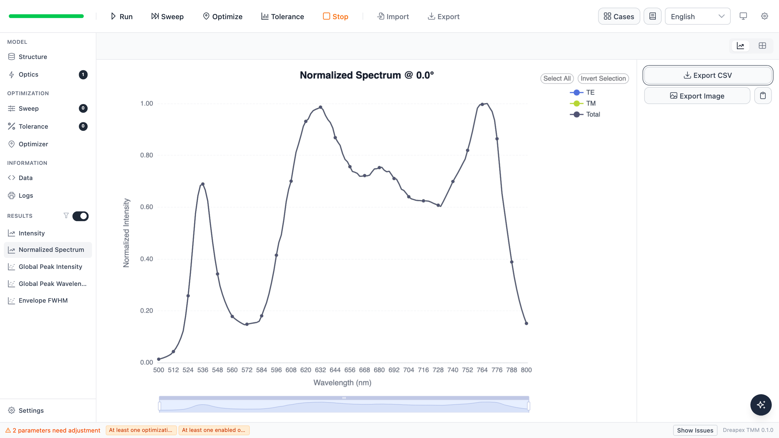
| Figure 4f | Normalized spectra of devices A, B, and C overlaid on one axis | Three Normalized Spectrum result pages | Split correspondence. Each screenshot covers one device; the software does not overlay separate models |
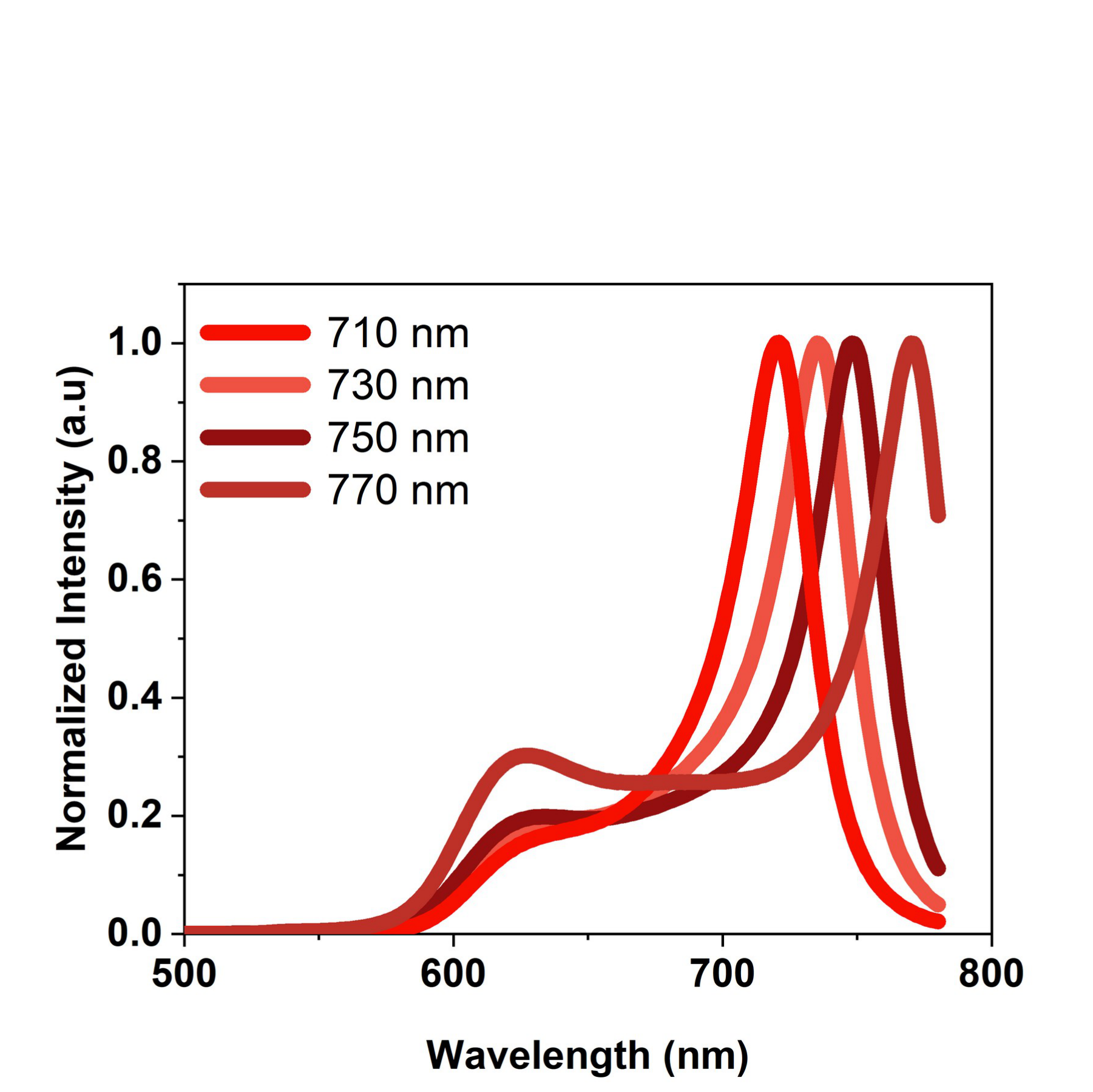
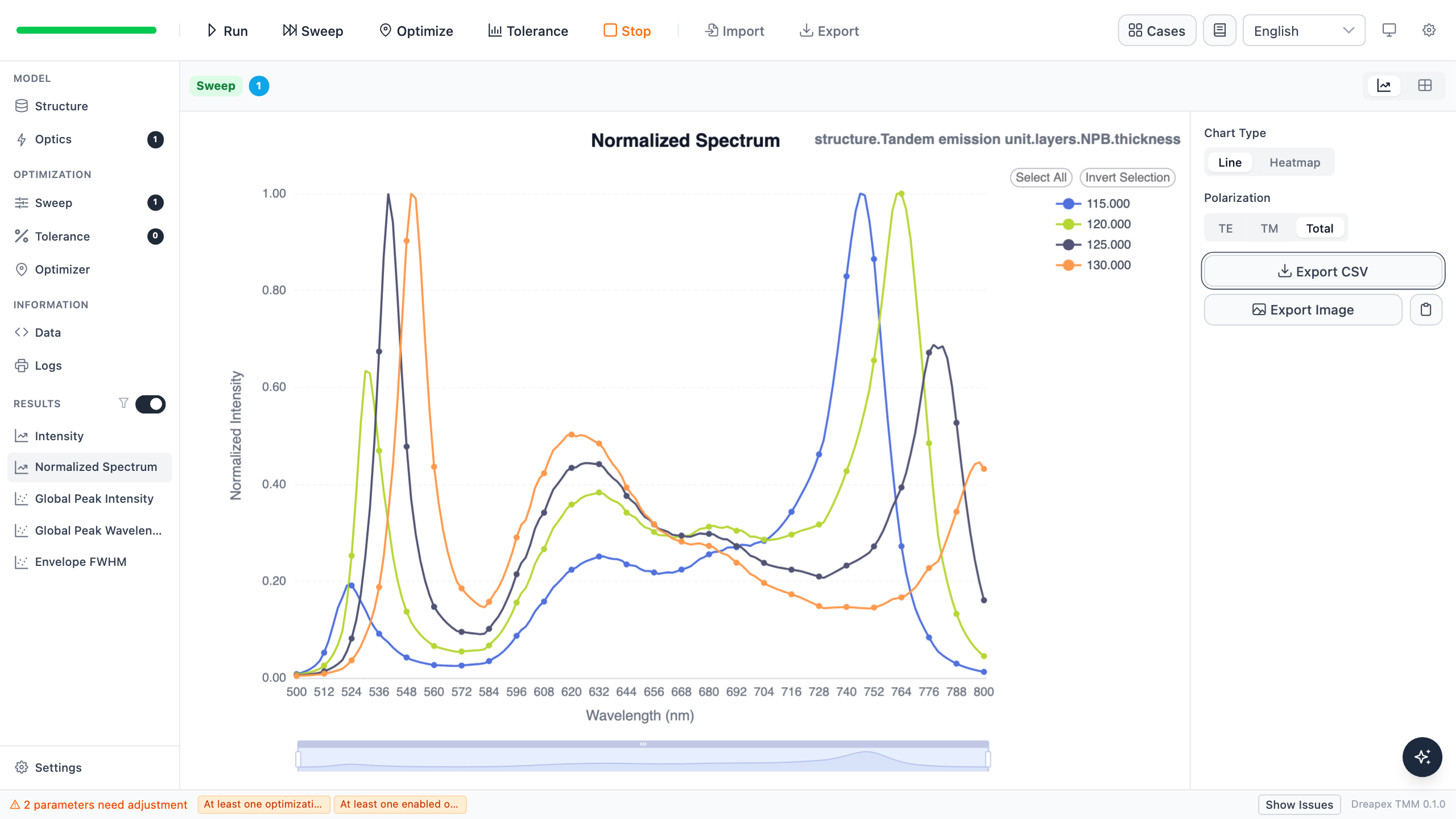
| Figure S16 | Normalized spectra of four target devices | One four-curve Normalized Spectrum sweep page | Direct chart-type correspondence. The scan parameters match, but the software does not produce the paper's four NIR main peaks |
Structure
Tandem microcavity devices B and C differ only in the Ag-anode thickness. Dreapex TMM Intensity calculates radiation toward the Top Medium end of the list. The software stack therefore starts on the emitting side with Glass substrate, followed by the Ag anode, two emission units, Liq, and the Al cathode. Both surrounding media are Air, and the 1 mm glass layer is marked Inco..
| Layer | Thickness | Layer state |
|---|---|---|
| Glass substrate | 1 mm | Inco. |
| Ag | Device B 30 nm; device C 20 nm | None |
| MoO₃ | 10 nm | None |
| NPB | 120 nm | None |
| Bebq₂:Ir(piq)₃ | 30 nm | Emis. |
| Alq₃:LiH | 40 nm | None |
| Liq | 1 nm | None |
| Al | 100 nm | None |
MoO₃, NPB, Bebq₂:Ir(piq)₃, and Alq₃:LiH form one Layer Group with Repeat Count set to 2. The Figure 3 and Figure S6 sweeps change the NPB and Alq₃:LiH thicknesses inside that group so that both emission units remain identical.

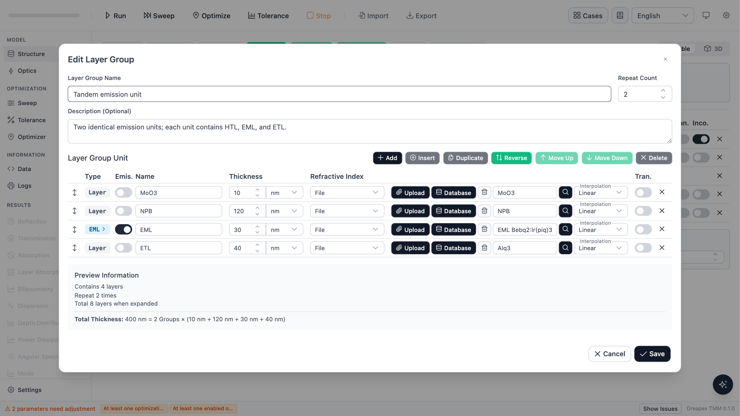
The non-cavity baseline replaces Ag with an assumed 150 nm ITO layer. NPB and Alq₃ are 40 nm and 20 nm in the single device; the non-cavity tandem device contains the same emission unit twice. Device A uses 30 nm Ag, 90 nm NPB, and 40 nm Alq₃ with one emission unit.
The paper's Methods give layer thicknesses and material names and state that and for every organic layer were measured by ellipsometry. The arrays are not published. This audit uses for glass and public dispersive entries from the Dreapex TMM refractive-index database for Ag, MoO₃, NPB, Alq₃, and Al. Transparent Alq₃ proxies for Bebq₂:Ir(piq)₃, and Alq₃:LiH uses the Alq₃ optical data. Neither refractive indices nor thicknesses were adjusted to register a paper peak.
Emitter and Sweep Settings
Each emissive layer contains an emitter at its centre with a Delta distribution, and the UI dipole-orientation field is set to Isotropic. The emission spectrum is extracted from the Ir(piq)₃ thin-film photoluminescence curve in paper Figure S1. The paper directly multiplies this normalized PL ordinate by its cavity gain and does not say whether the spectrum is photon counts or radiant power, so it is entered as Power here. The two tandem emission units have equal weights; quantum efficiency, conversion efficiency, and multiplier are all 1.
| Setting | Value |
|---|---|
| Detector | Emission Intensity |
| Emission angle | Single, 0° |
| Figures 1c and 4f | 400–800 nm or 500–800 nm, 2 nm step |
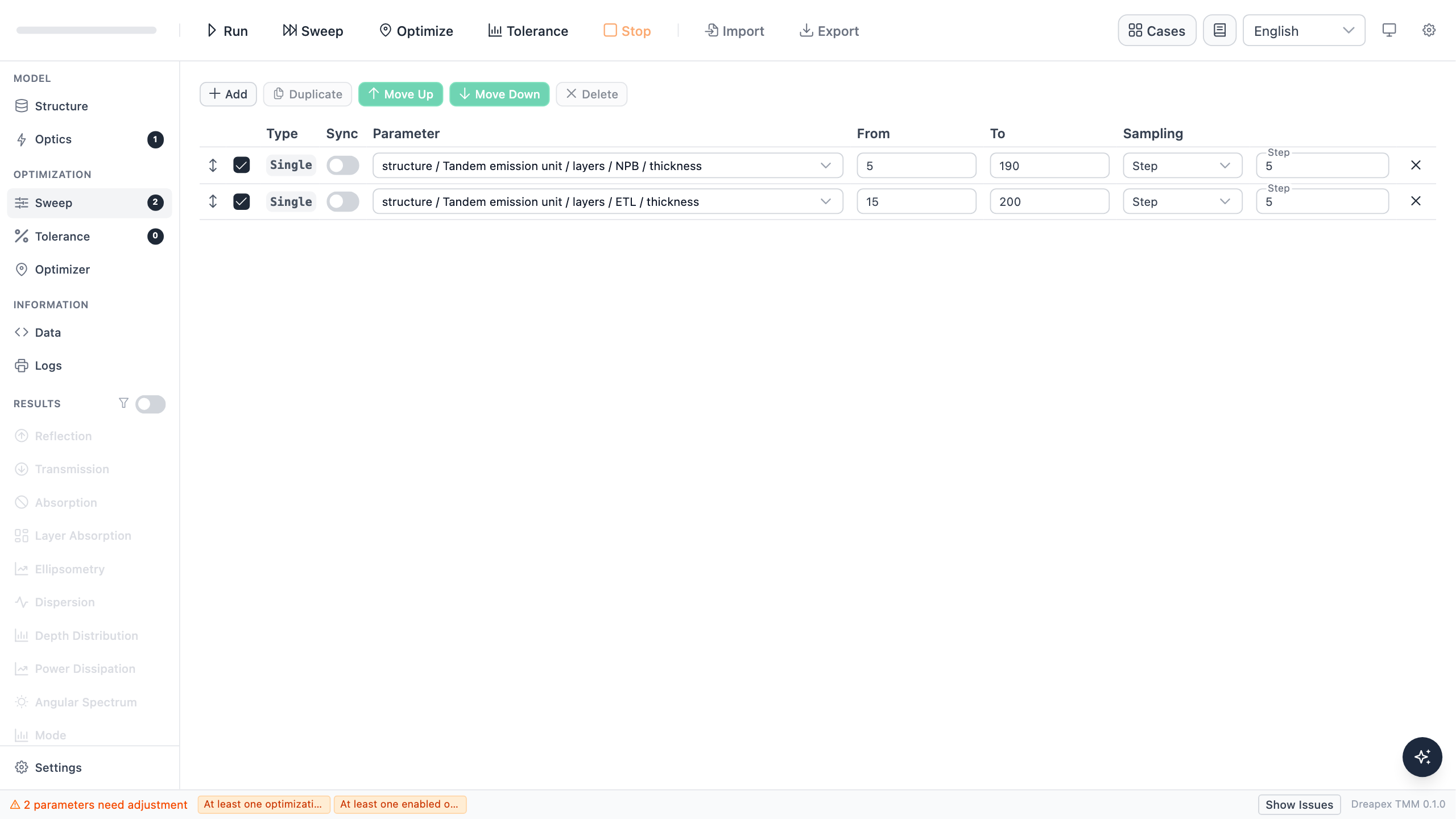
| Figure S8 | Ag 15–40 nm, 5 nm step; wavelength 550–800 nm, 2 nm step |
| Figure S16 | Per-unit NPB 115–130 nm, 5 nm step; wavelength 500–800 nm, 2 nm step |
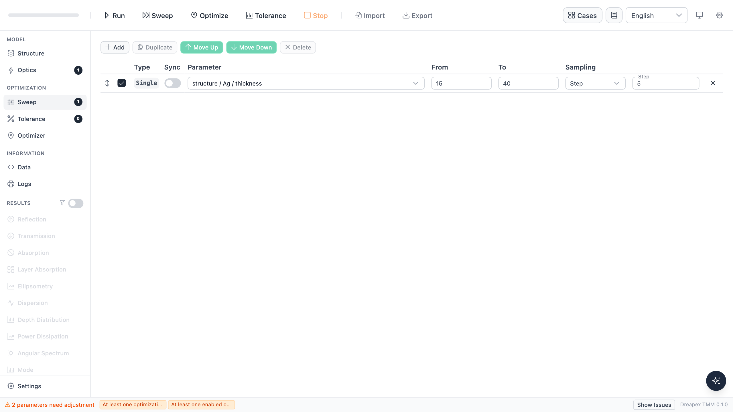
| Figure 3 | Per-unit NPB 5–140 nm and ETL 5–50 nm, both in 5 nm steps; single target wavelength |
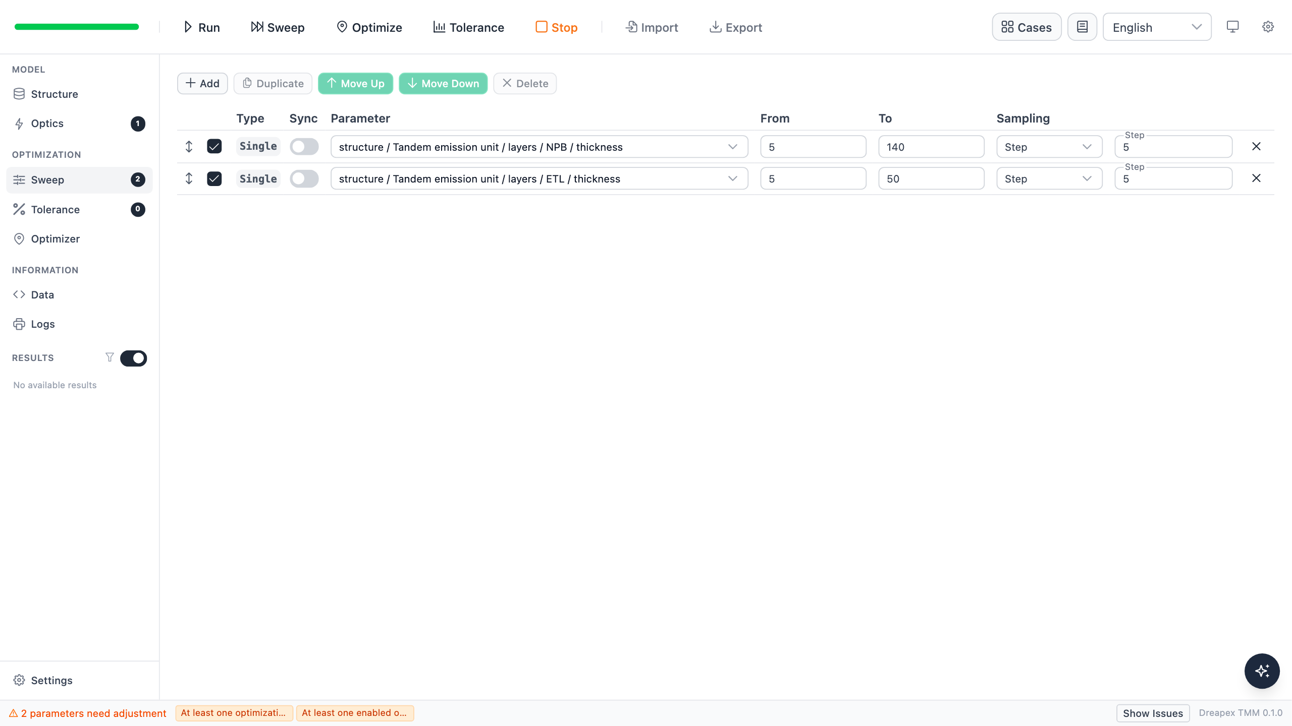
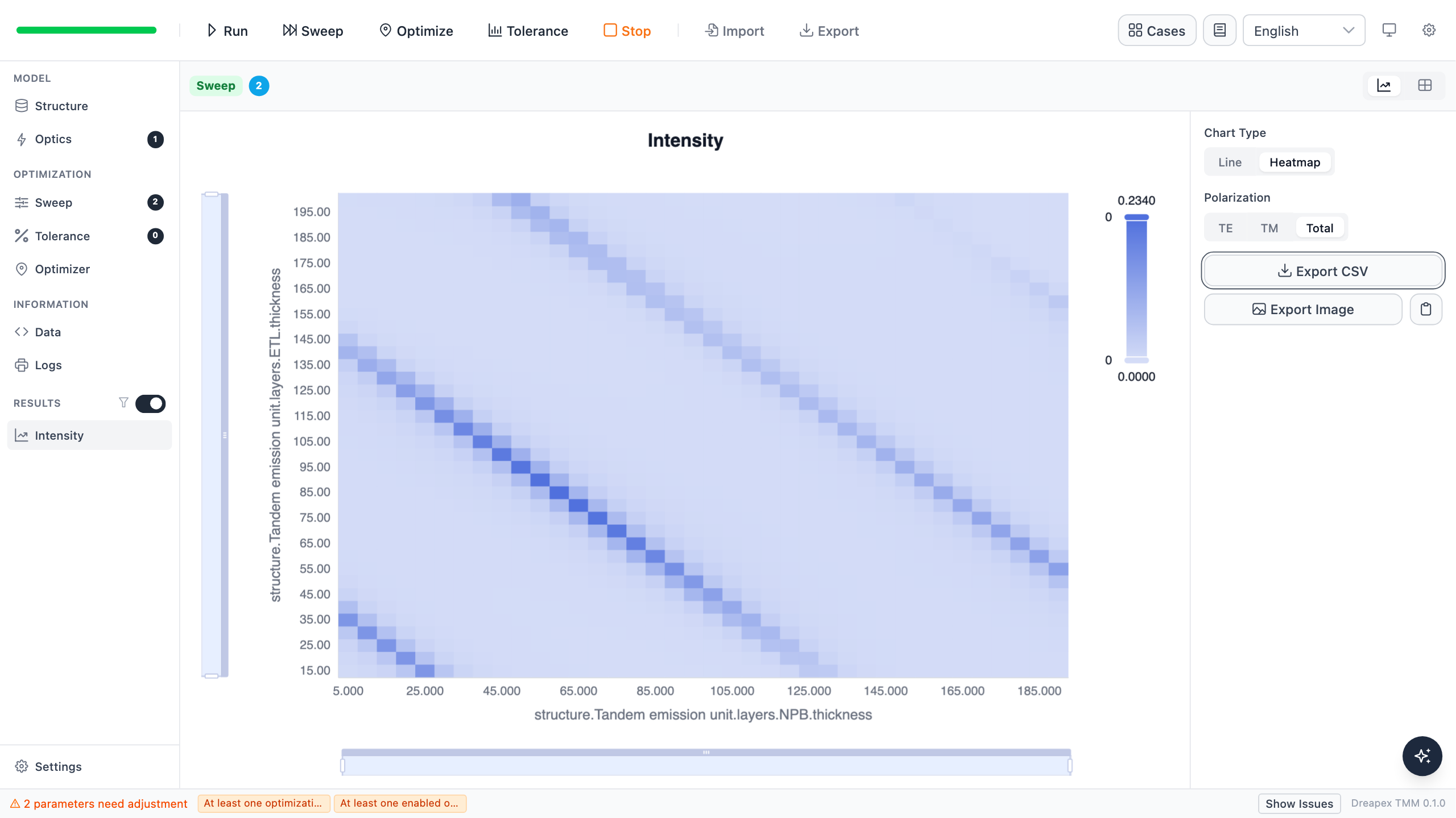
| Figure S6 | Per-unit NPB 5–190 nm and ETL 15–200 nm, both in 5 nm steps; single target wavelength |

The four software sweep configurations follow. Total, Line, and Heatmap are selected later on the result pages.

Non-Cavity Normalized Spectra (Figure 1c)
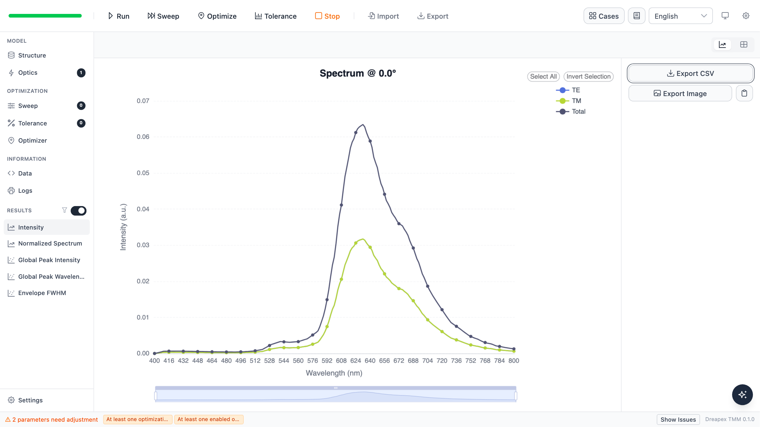
Figure 1c gives measured normalized electroluminescence spectra for the single and tandem non-cavity devices, with the paper's own optical simulations overlaid. The measured single-device peak is 630.1 nm. The tandem peak is 626.4 nm, with a broader long-wavelength shoulder.
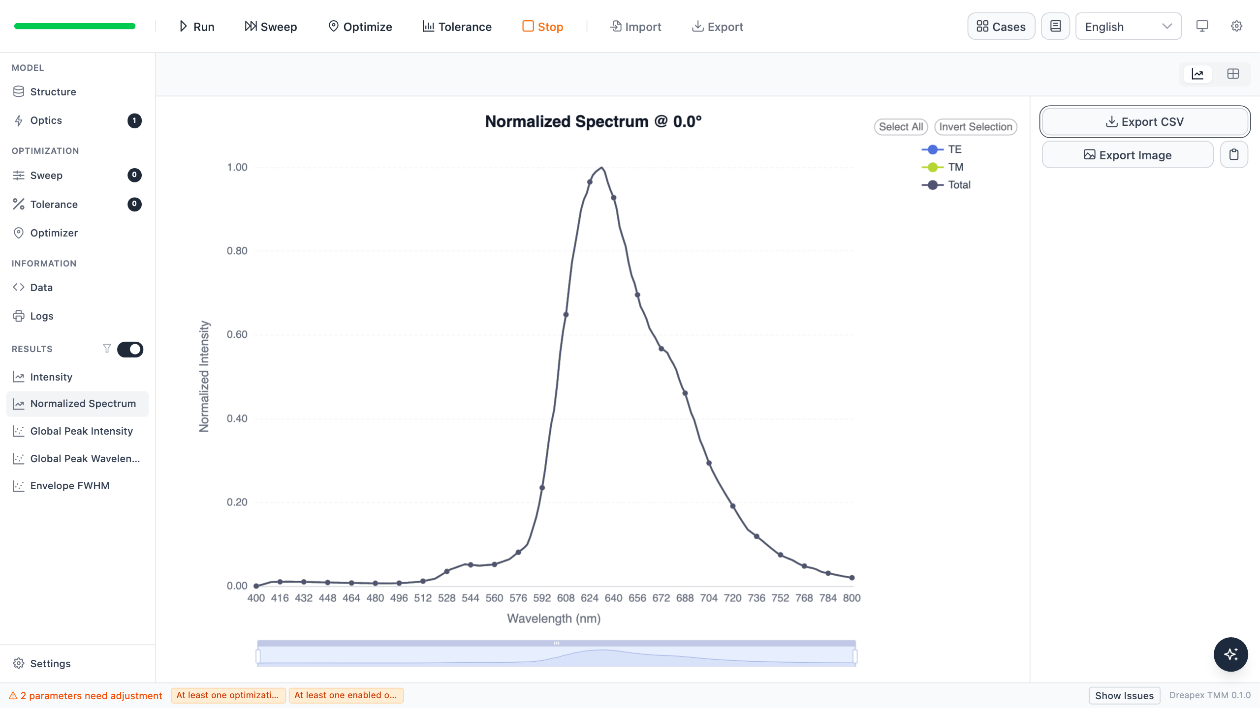
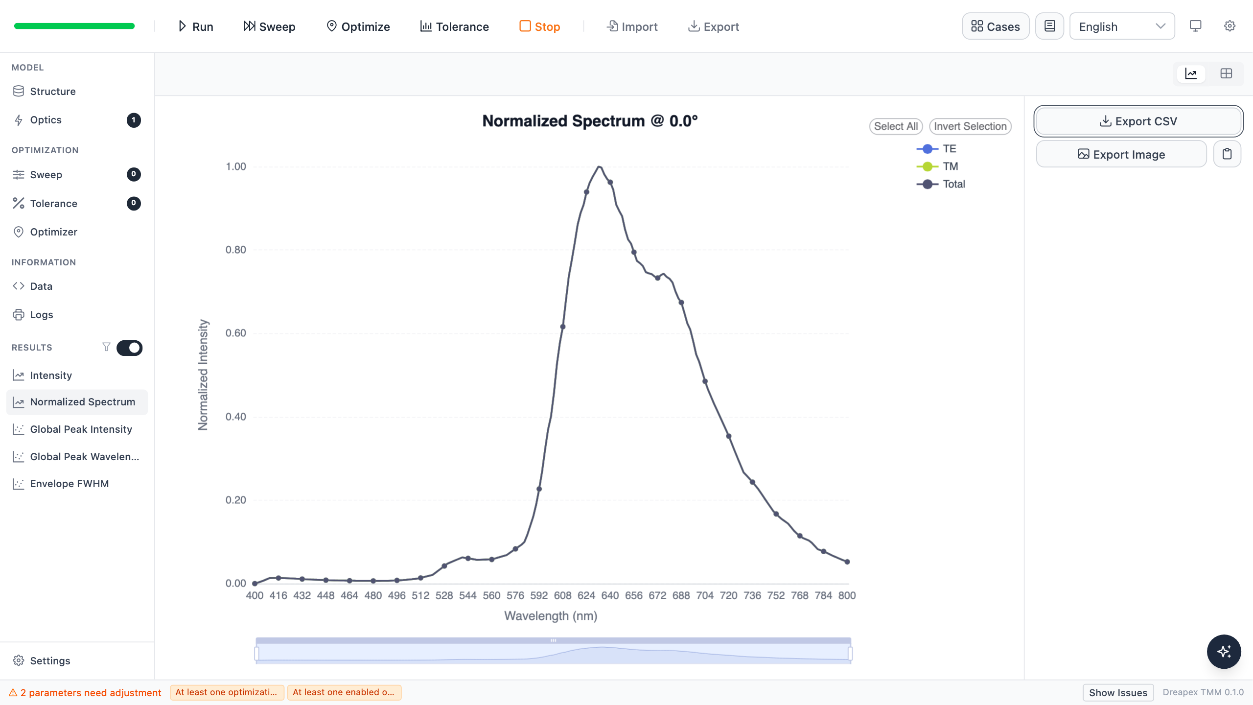
| Quantity | Paper measurement | Dreapex TMM | Difference |
|---|---|---|---|
| Single-device peak | 630.1 nm | 631.7 nm | +1.6 nm |
| Single-device envelope FWHM | 88.0 nm | 80.9 nm | −7.1 nm |
| Single-device normalized lineshape RMS | Not applicable | 8.1% | Not applicable |
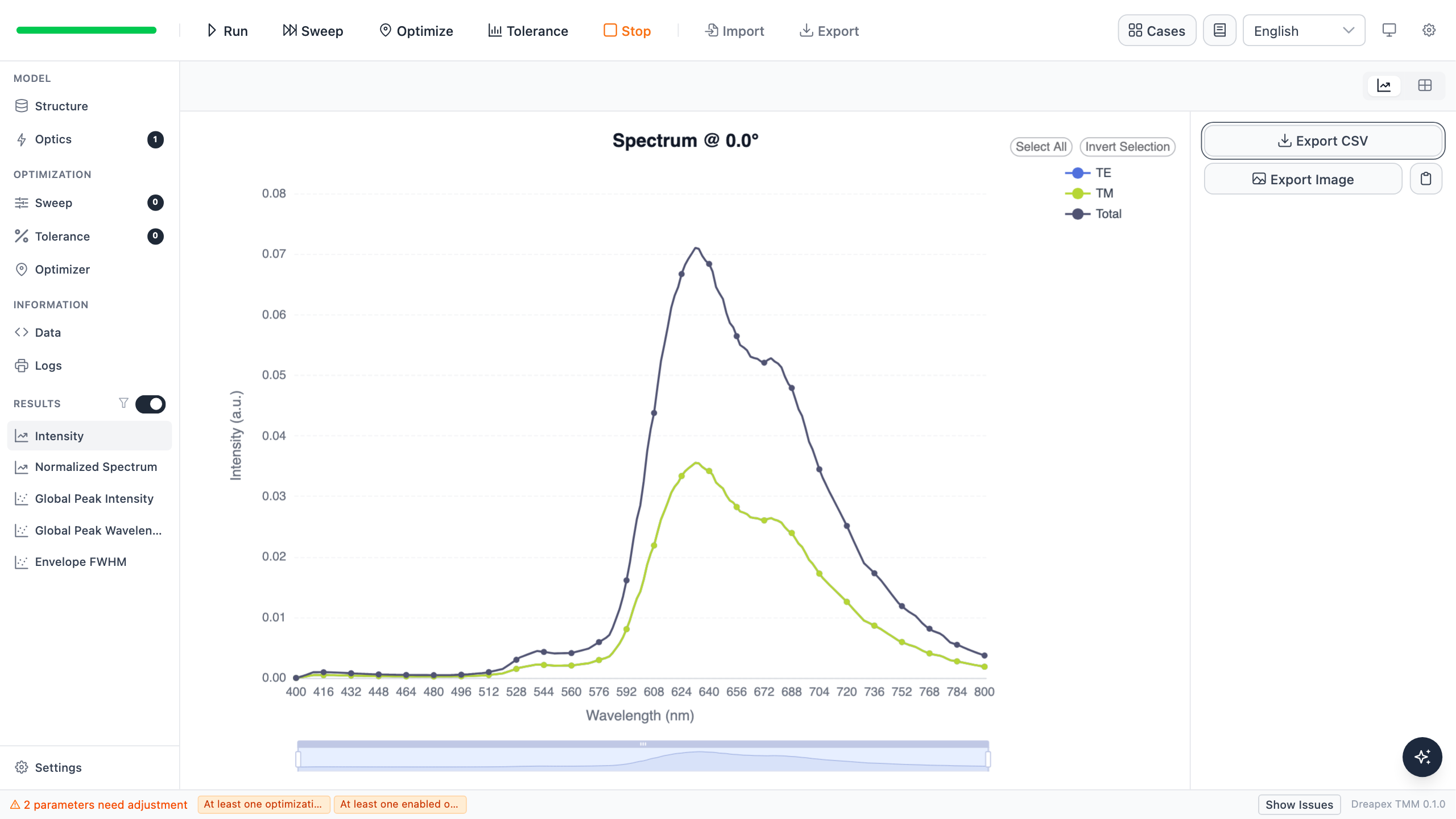
| Tandem-device peak | 626.4 nm | 632.7 nm | +6.3 nm |
| Tandem-device envelope FWHM | 102.6 nm | 99.5 nm | −3.1 nm |
| Tandem-device normalized lineshape RMS | Not applicable | 4.1% | Not applicable |
The RMS values compare the extracted paper measurement and the exported normalized software intensity point by point over 580–778 nm. The two screenshots address the Single and Tandem objects in Figure 1c separately; this split presentation is not the same as reproducing the paper's four-curve layout.
Final Intensity and Decomposition Boundary (Figure S4)
Figure S4 separates the paper model into PL, Fabry–Pérot factor, two-beam factor, and final intensity. Dreapex TMM Intensity reports the complete emission intensity and does not expose the first three paper-specific factors as separate result charts. The two software screenshots below therefore correspond only to the final Intensity curve in each Figure S4 panel.
Coordinate Conversion for the 2D Cavity Maps
Figures 3 and S6 use the total thicknesses of the two HTLs and two ETLs in the tandem cavity. A software Layer Group sweep varies the NPB and ETL thickness in one emission unit, so the paper coordinates and relate to the software inputs as
Here, is the paper's total HTL thickness, is its total ETL thickness, and and are the NPB and ETL thicknesses in one emission unit. The fixed 10 nm is the MoO₃ layer in each unit. Every thickness is in nm. Each paper panel below sits immediately before the software screenshot with the same wavelength and scan range.
Design-Window Cavity Maps (Figure 3)
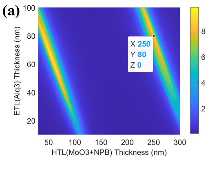
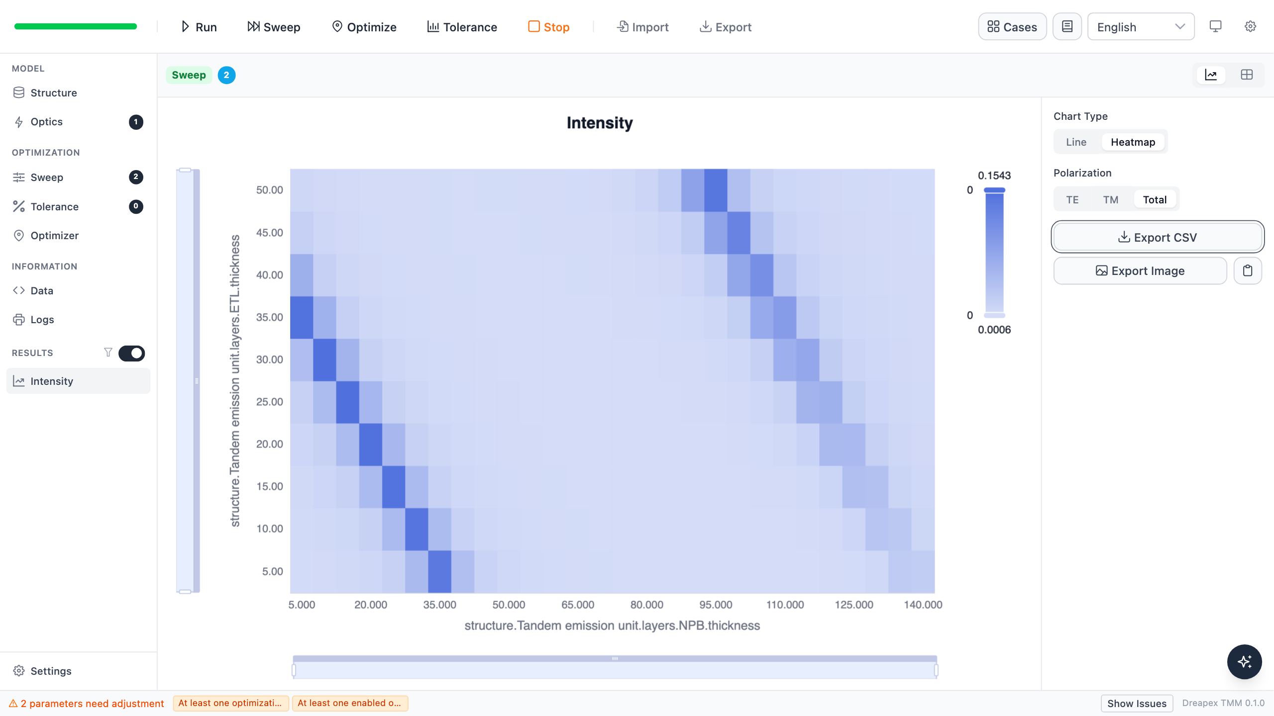
Figure 3 spans approximately 30–300 nm total HTL and 10–100 nm total ETL. The matching software sweep uses per-unit NPB 5–140 nm and ETL 5–50 nm. The four marked paper design points map to per-unit NPB values of 115, 120, 125, and 130 nm, respectively, with ETL fixed at 40 nm.
710 nm: Figure 3a
730 nm: Figure 3b
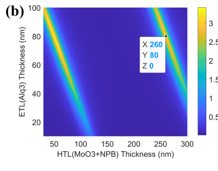
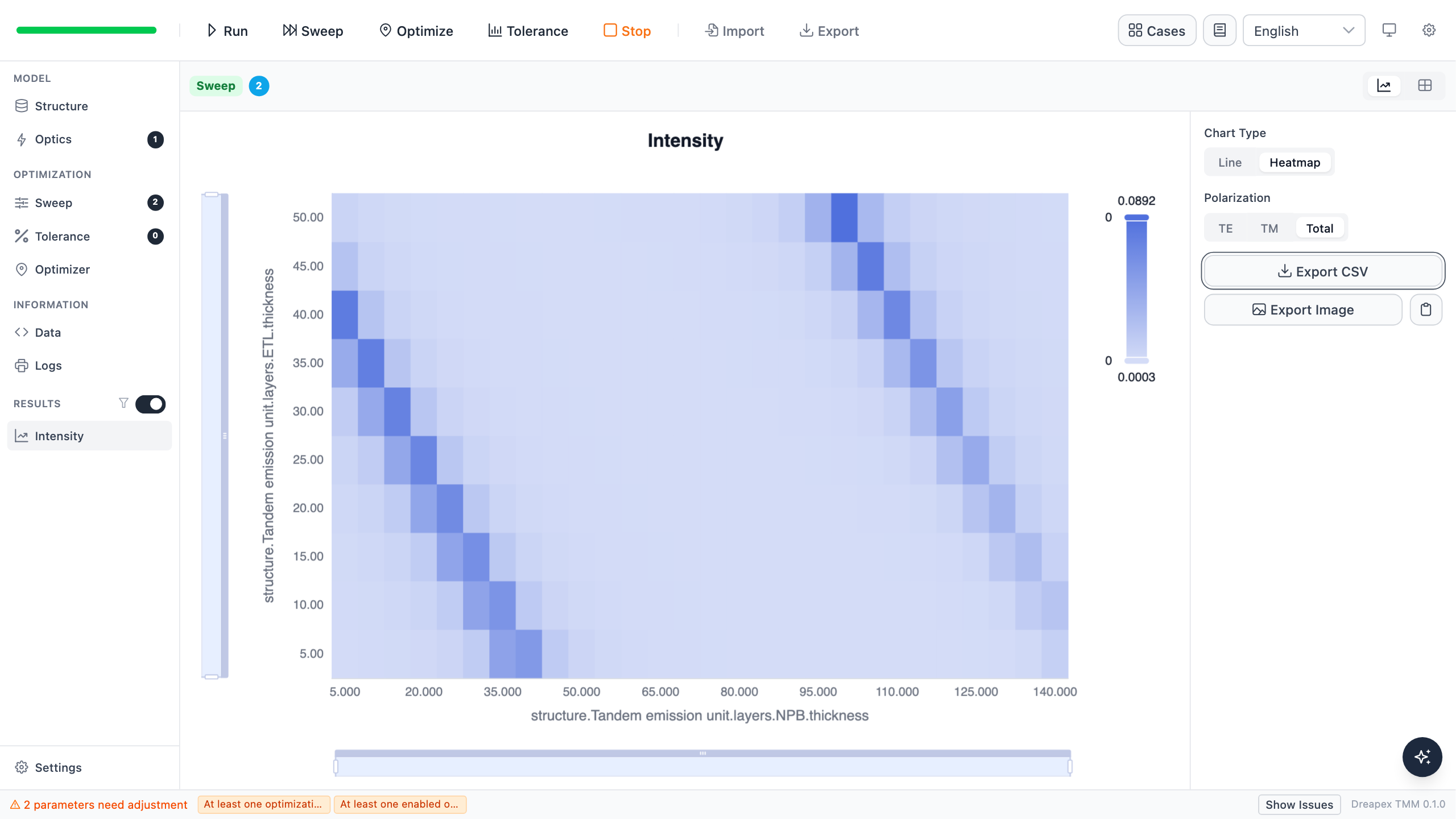
750 nm: Figure 3c
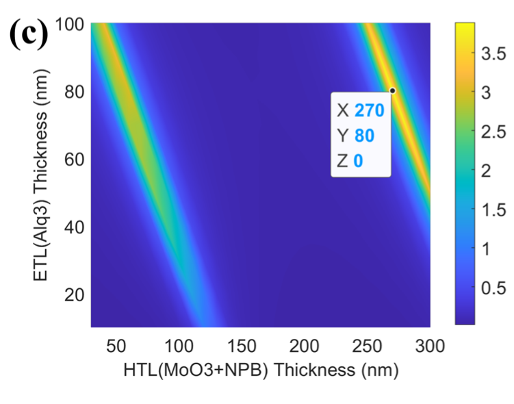
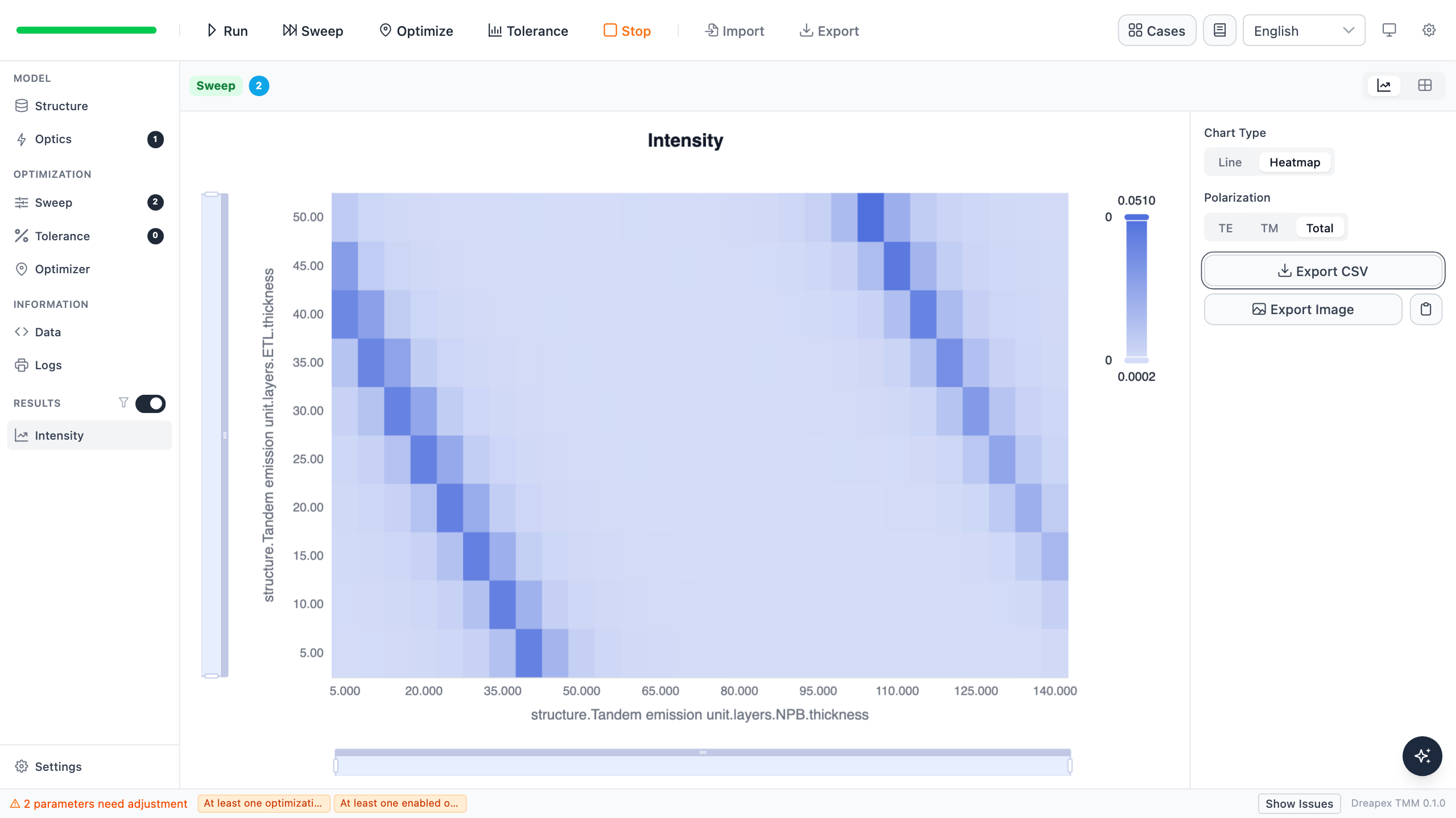
770 nm: Figure 3d
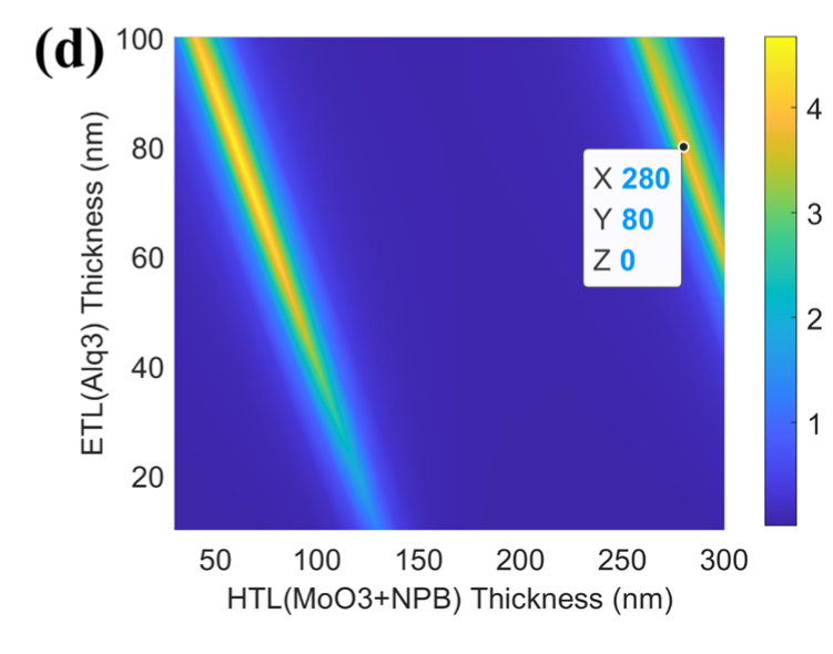
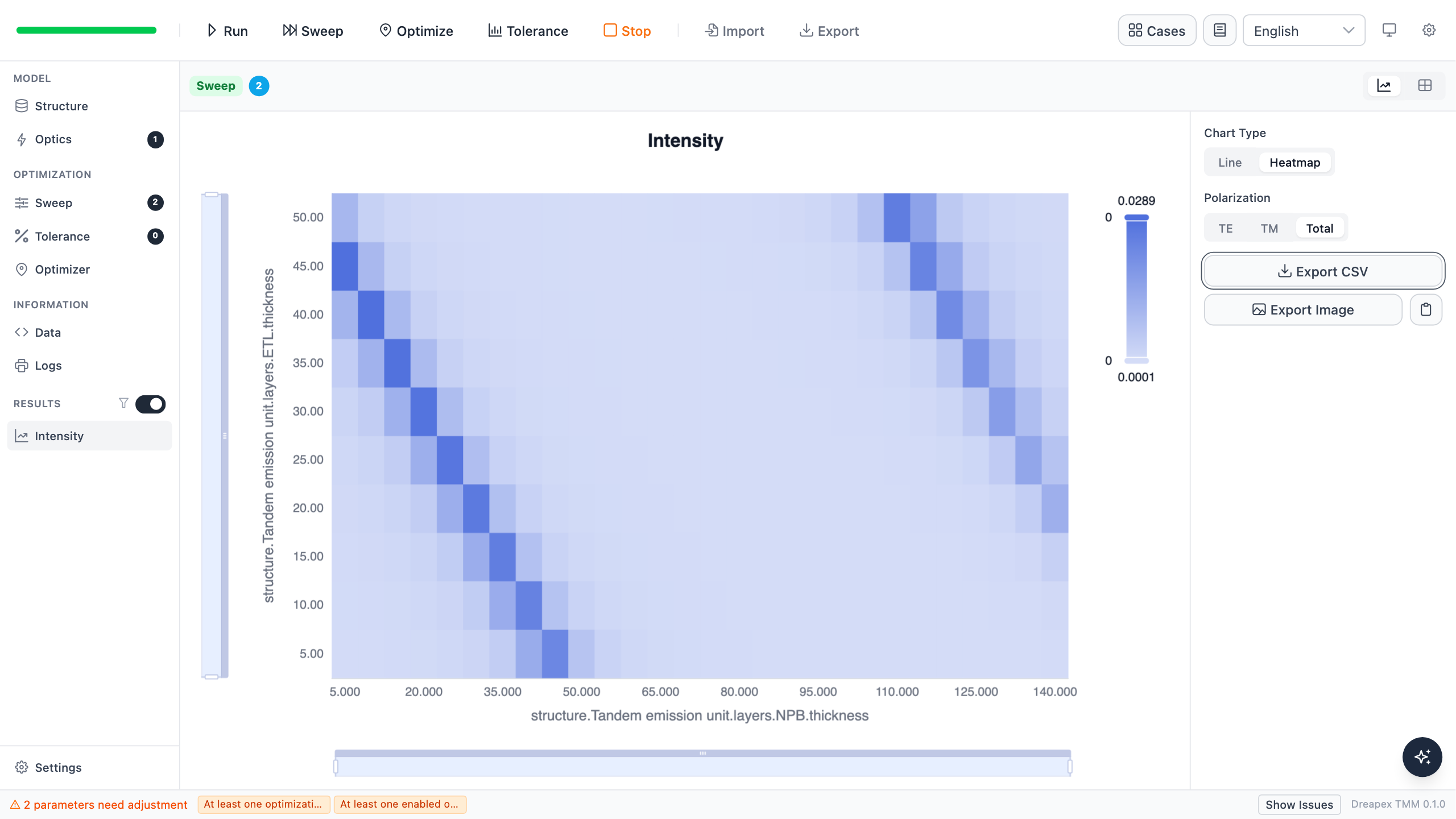
All four software maps and Figures 3a–d contain two bright ridges that descend from left to right, and both ridges shift toward thicker NPB as the target wavelength increases. Their absolute positions do not land on the marked paper points. At a paper total ETL thickness of 80 nm, the right-hand ridge near the design point gives:
| Target wavelength | Paper total HTL | Dreapex TMM total HTL | Difference |
|---|---|---|---|
710 nm | 250 nm | 227.9 nm | −22.1 nm |
730 nm | 260 nm | 239.4 nm | −20.6 nm |
750 nm | 270 nm | 250.2 nm | −19.8 nm |
770 nm | 280 nm | 261.0 nm | −19.0 nm |
Wide-Range Cavity Maps (Figure S6)
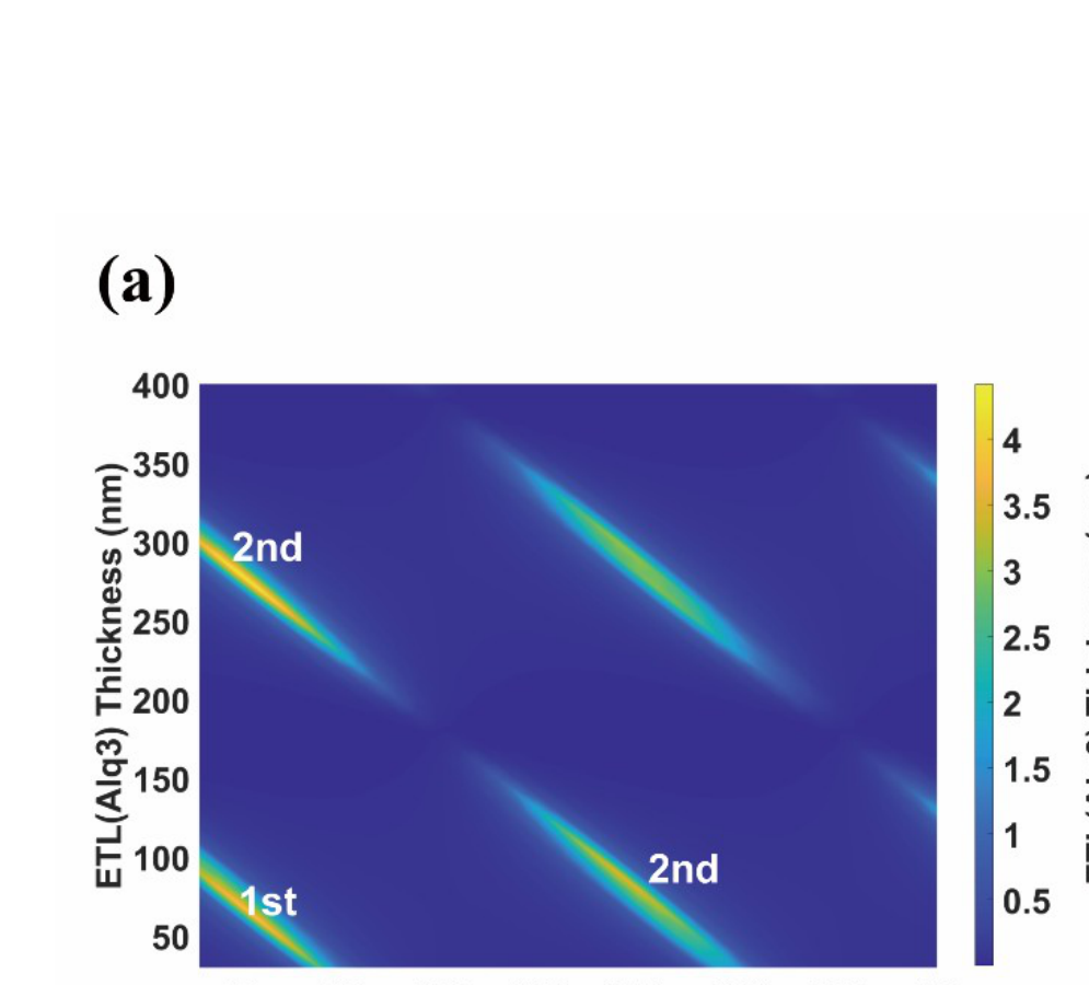
Figure S6 extends both total HTL and total ETL to 30–400 nm. The software uses per-unit NPB 5–190 nm and ETL 15–200 nm, which map to the same total-thickness ranges. The four pairs below retain the one-panel-to-one-screenshot order.
710 nm: Figure S6a
730 nm: Figure S6b
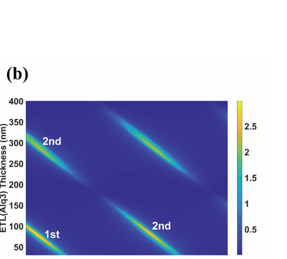
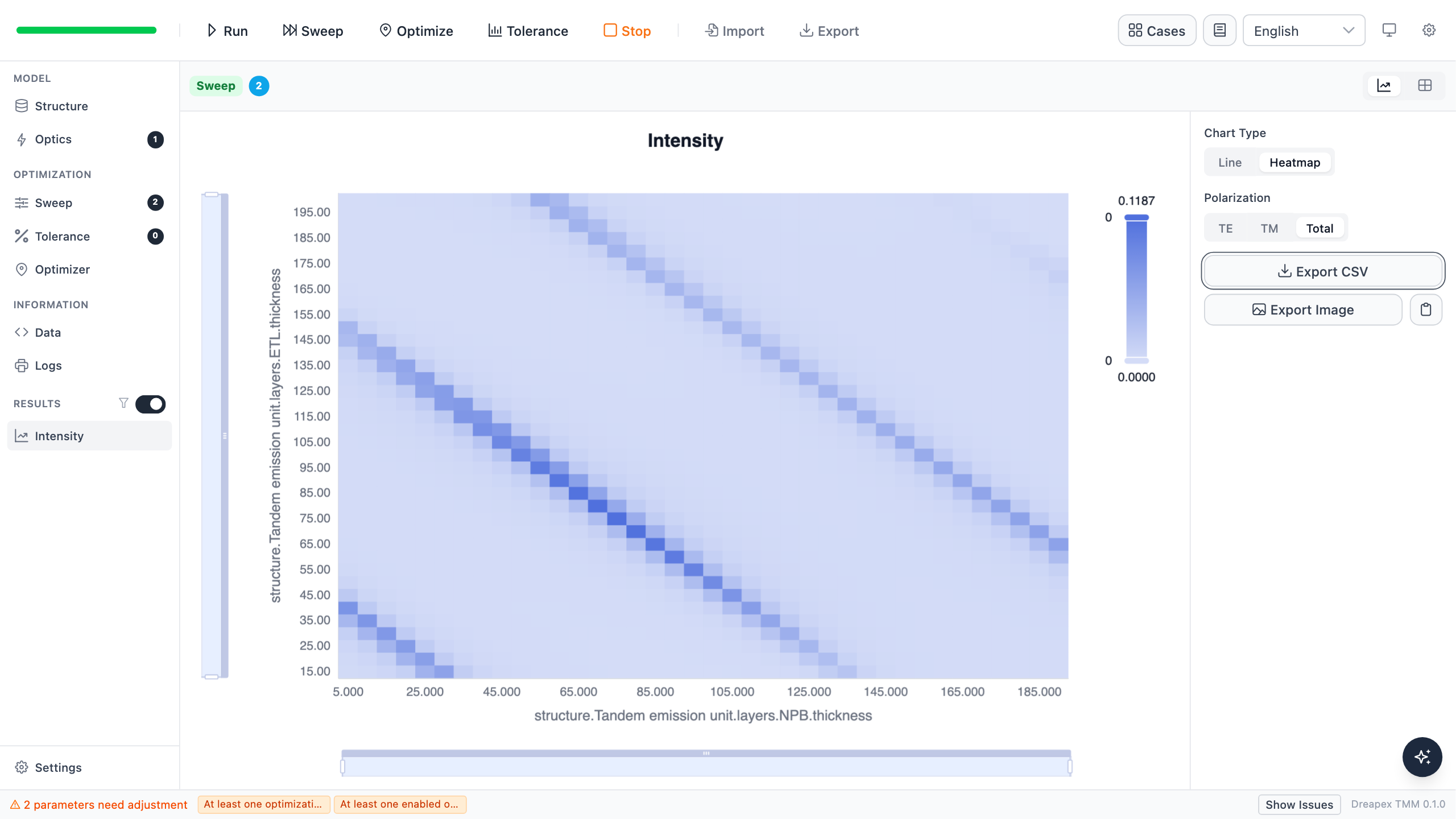
750 nm: Figure S6c
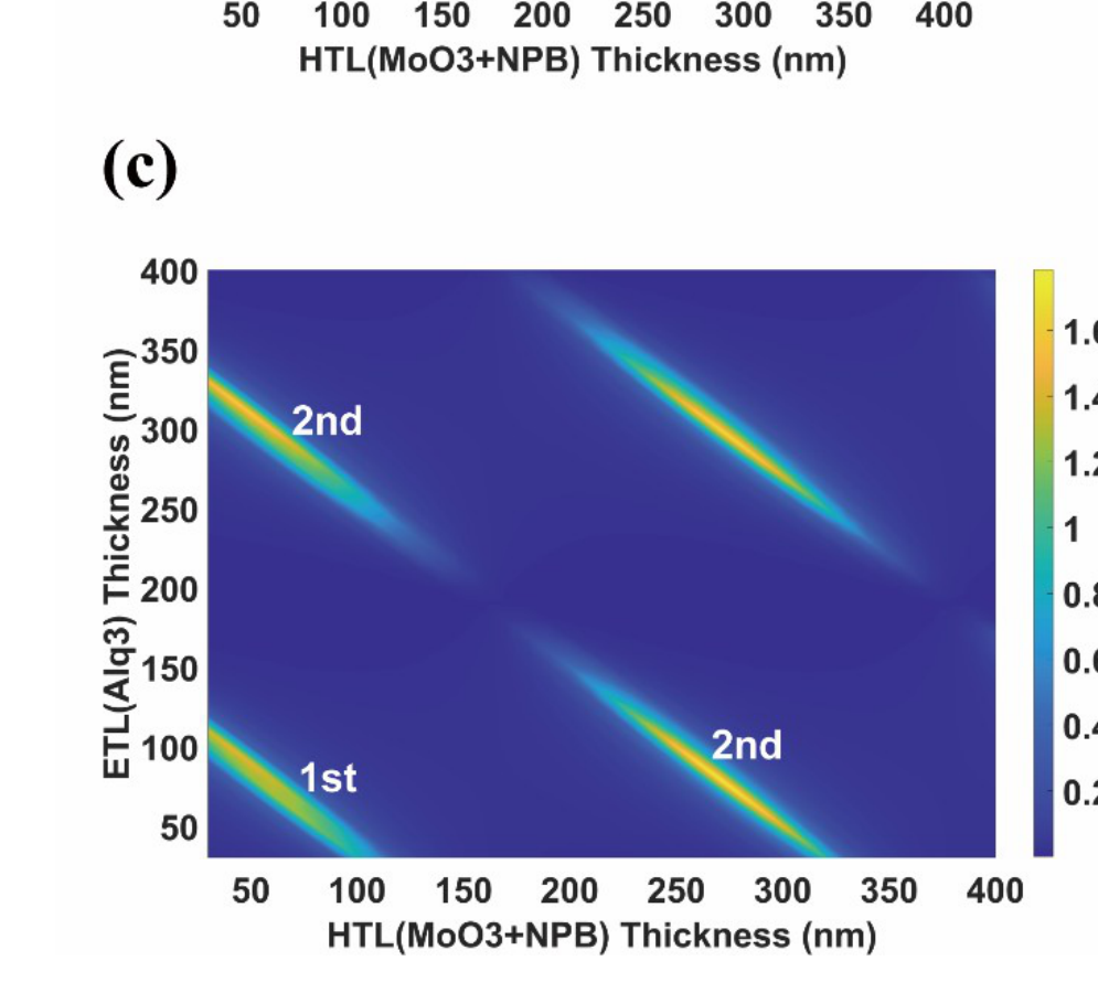
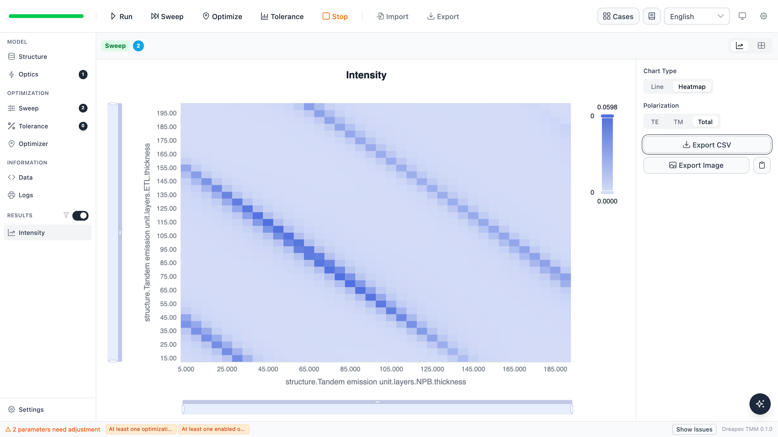
770 nm: Figure S6d
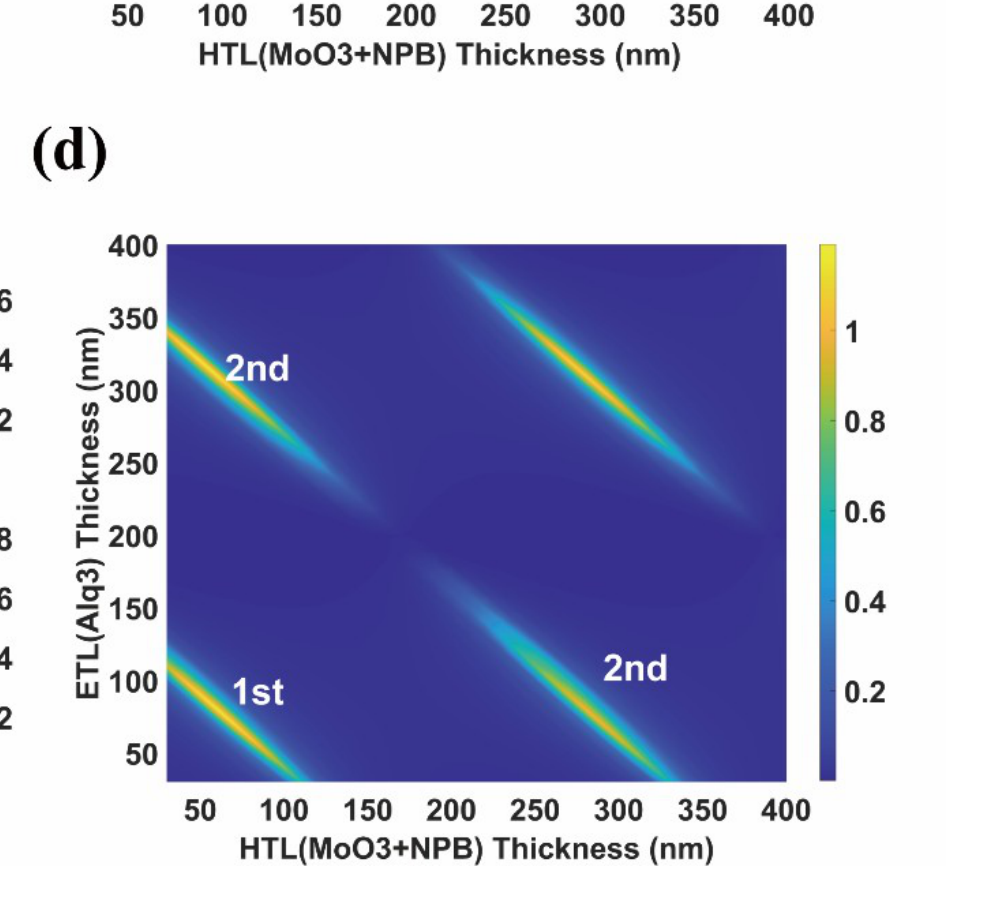
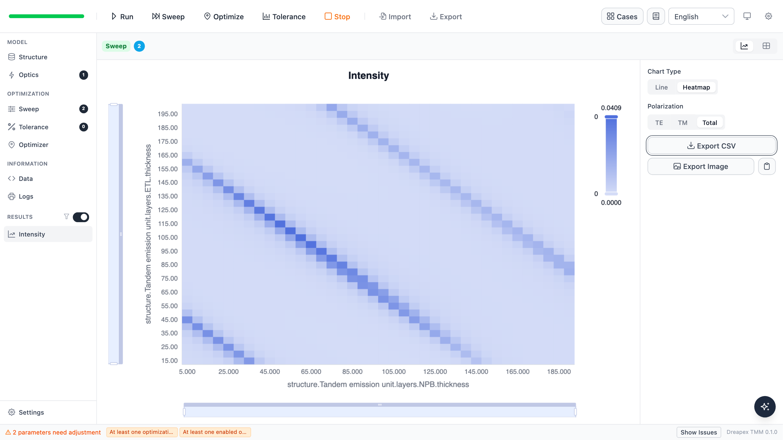
With all eight Figure S6 images aligned by wavelength, Dreapex TMM reproduces the number of mode-ridge families, their slope, and their red-shift direction. The absolute ridge coordinates retain a 19.0–22.1 nm total-HTL difference.
Ag Thickness and Figure S8
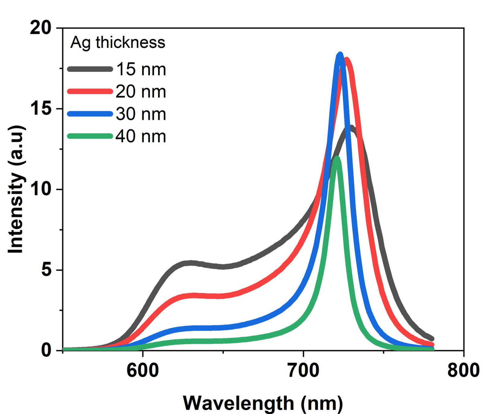
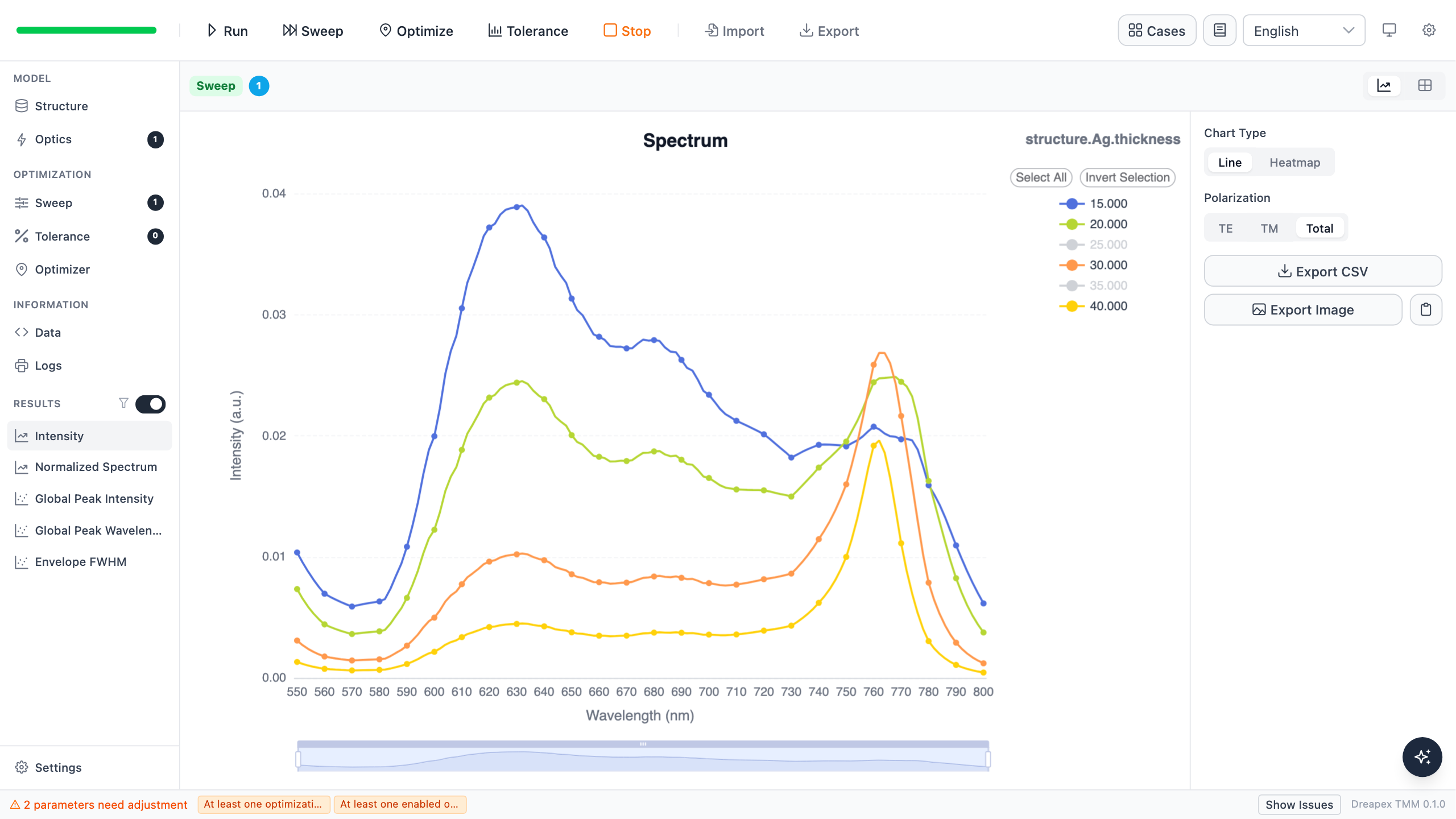
Paper Figure S8 changes the Ag anode in the same tandem cavity to 15, 20, 30, and 40 nm. The paper curves narrow as Ag becomes thicker. Their NIR peak intensity first rises, reaches its maximum at 30 nm, and then falls at 40 nm.
| Ag thickness | Paper relative NIR peak | Dreapex TMM | Paper FWHM | Dreapex TMM envelope FWHM |
|---|---|---|---|---|
15 nm | 0.754 | 0.773 | 60 nm | 124.2 nm |
20 nm | 0.983 | 0.926 | 30 nm | 184.3 nm |
30 nm | 1.000 | 1.000 | 19 nm | 30.6 nm |
40 nm | 0.649 | 0.731 | 14 nm | 21.5 nm |
Each relative-intensity set is normalized to its own 30 nm result, giving four differences between 0.000 and 0.082. The software result also shows stronger NIR narrowing with thicker Ag. The 15 nm and 20 nm results contain broad lobes absent from the paper, so their envelope FWHM values do not describe the same isolated peak.
Devices A/B/C and Figure 4f
Figure 4f gives measured normalized electroluminescence spectra for three finished devices. A has one emission unit and 30 nm Ag. B has two units and 30 nm Ag. C has two units and 20 nm Ag. Their published peaks are 727, 727, and 732 nm.
| Device | Paper peak | Dreapex TMM peak | Peak difference | Paper FWHM | Dreapex TMM envelope FWHM |
|---|---|---|---|---|---|
| A | 727 nm | 724.1 nm | −2.9 nm | 52 nm | 74.5 nm |
| B | 727 nm | 763.0 nm | +36.0 nm | 23 nm | 30.6 nm |
| C | 732 nm | 767.2 nm | +35.2 nm | 34 nm | 184.3 nm |
The absolute peak of device A is close to the paper, while its linewidth is 22.5 nm larger. The NIR main peak of B is substantially red-shifted. C has several strong lobes and stays above half maximum over a broad interval, so its 184.3 nm envelope width does not represent the isolated NIR peak reported in the paper.
Target-Wavelength Devices and Figure S16
Paper Figure S16 gives measured devices targeting 710, 730, 750, and 770 nm. Paper Table 1 assigns per-unit NPB thicknesses of 115, 120, 125, and 130 nm, respectively, with a fixed 40 nm ETL.
| Paper target peak | Per-unit NPB | Dreapex TMM NIR local peak | Difference | Local peak relative to global peak |
|---|---|---|---|---|
710 nm | 115 nm | 746.8 nm | +36.8 nm | 1.000 |
730 nm | 120 nm | 763.0 nm | +33.0 nm | 1.000 |
750 nm | 125 nm | 778.4 nm | +28.4 nm | 0.688 |
770 nm | 130 nm | 797.5 nm | +27.5 nm | 0.445 |
The software results preserve the red-shift order of the NIR local peak as NPB becomes thicker. The global peaks of the 750 nm and 770 nm models are at 540.4 and 550.8 nm, so the NIR features shown in the screenshot are only local peaks. This differs from the four NIR main peaks in the paper.
Deviation Boundaries
- The measured organic-layer and are absent from the publication. The
19.0–22.1 nmFigure S6 thickness differences and the approximately35 nmtandem-device peak differences both indicate an optical-thickness mismatch; the current evidence cannot assign it uniquely to one material. - Alq₃ proxies for Bebq₂:Ir(piq)₃, and Alq₃:LiH also uses Alq₃ data. These proxies preserve the basic cavity behaviour of transparent organic layers but not the measured dispersion of the paper samples.
- The paper does not give the relative emission strengths or actual recombination positions of the two emission units. This audit uses equal weights at both layer centres; both quantities change the combined tandem spectrum.
- The paper equations first add the Fabry–Pérot terms of the two units and separately add their two-beam terms before multiplying those sums. Dreapex TMM calculates the radiation from each emissive layer and then adds the two contributions. These definitions can assign different weights to lobes in a strong microcavity.
- Agreement in the Figure S8 relative NIR-intensity trend does not establish agreement of the complete spectra. The matching Figure S6 mode shape also does not replace the absolute-coordinate check.
This page retains the unresolved results so that the publication figures can be compared directly with the software result pages. If the measured organic-layer ellipsometry data become available, the same layer thicknesses, emission positions, and sweep grids can be rerun to test the absolute tandem-microcavity peaks.
Back to Case Studies · Next: Bidirectional Vertical Radiance Ratio of a Transparent Perovskite LED