Purcell-Factor Spectrum of a Top-Emitting OLED Capping Layer
Importance of Purcell factor for optimizing structure of organic light-emitting diodes
Authors: Hyunsu Cho, Jin Chung, Jinouk Song, Jaeho Lee, Hyunkoo Lee, Jonghee Lee, Jaehyun Moon, Seunghyup Yoo, and Nam Sung Cho
Journal: Optics Express 27(8), 11057–11068 (2019) · Comparison target: Figure 5
Deposit one more film on the outside of a semi-transparent OLED electrode and the spontaneous emission rate of the emitter changes — even though that film carries no current at all.
This case builds four top-emitting devices that differ only in capping-layer thickness (0, 30, 60, and 90 nm of NPB) and runs a 400–700 nm Mode sweep on each, producing the same chart the paper shows: the Purcell factor across the full wavelength axis.
All four top-emitting curves rise to F ≈ 2.1–2.5 around 480–520 nm, then fall back towards 1.4 at long wavelengths. The uncapped device has the highest peak and the 30 nm device the lowest.
Background
The Purcell factor states how much a layered optical environment changes the radiative decay rate of a dipole:
is the dimensionless Purcell factor, the vacuum wavelength, the radiative decay rate inside the OLED cavity, and the corresponding free-space radiative decay rate; both rates are in . A value above one means the cavity raises the total radiative decay rate at that wavelength; it does not mean the same proportion of power escapes into air.
Both metal interfaces of this device — the 25 nm Ag top electrode and the opaque Al bottom mirror — are strongly reflective. The NPB capping layer sits outside the electrically active stack, but its thickness changes the reflection phase at the semi-transparent electrode and therefore moves the peak position and peak height of the whole curve.
Structure
Layers run from the air side to the glass. Complex indices are written as and are all fixed at their 520 nm values.
| Layer | Thickness | Optical input |
|---|---|---|
| NPB capping layer | 0, 30, 60, or 90 nm | Open quartz-film sample of the same material, , |
| Ag semi-transparent electrode | 25 nm | Ciesielski 20 nm Ag/SiO₂ open film data, , |
| LiF / Al electron-injection bilayer | 1 / 2 nm | LiF , ; open Al , |
| BmPyPB electron-transport layer | 50 nm | BPhen quartz-film proxy, , |
| 26DCzPPy:Ir(ppy)₃ emissive layer | 10 nm | mCBP quartz-film proxy, , |
| TCTA:Ir(ppy)₃ emissive layer | 10 nm | Open quartz-film sample of the same material, , |
| TAPC hole-transport layer | 40 nm | Open quartz-film sample of the same material, , |
| HAT-CN hole-injection layer | 10 nm | HAT-CN6 quartz-film sample, , |
| Al bottom mirror | 100 nm | Same open Al input as the 2 nm layer |
| Glass substrate | Semi-infinite boundary | , |
The uncapped variant simply omits the first row; no zero-thickness layer is added:

With 30 nm of NPB added, only the first row changes:

60 nm:

90 nm, with the electrically active OLED stack still identical to the previous three:

Optical and Emitter Settings
The paper confines recombination to the interface between the two 10 nm emissive sublayers but does not state which material's local optical environment an interfacial dipole belongs to. This case places one Delta emitter on each side of the interface with a weight of 0.5 each, and reports as their equal-weight mean.
| Emission setting | Value |
|---|---|
| Calculation wavelengths | 400–700 nm, 5 nm step, 61 wavelengths |
| Source spectrum | Unit White ( is computed per wavelength and does not depend on the source spectral shape) |
| Dipole distribution | Delta on each side of the interface, 0.01 nm from it, weight 0.5 each |
| Dipole orientation | Isotropic |
| Intrinsic quantum efficiency | 0.8 |
| Detector | Mode |
| Comparison quantity | Emitter-level Purcell factor |
The 26DCzPPy-side emitter, at relative position 0.999:

The symmetric emitter on the TCTA side, at relative position 0.001:

Only Mode is enabled, with the wavelength mode switched to Sweep over the paper's horizontal axis:

Optimize.Simulation Results and Comparison with Figure 5
Paper Figure 5 carries six curves; the four filled-circle series are the top-emitting devices reproduced here. View it in the original article.
Values read from the four published curves and the 61-wavelength run of this case, drawn on one axis in the paper's colours:
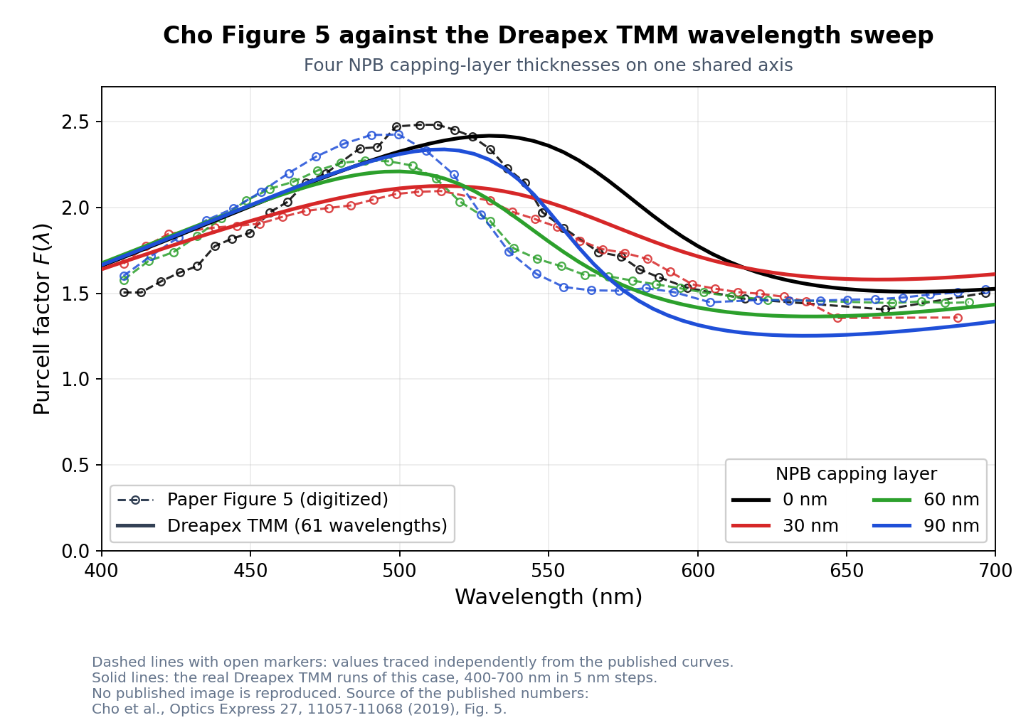
The peak heights rank the same way as in the paper: 0 nm highest, then 90 nm, then 60 nm, with 30 nm lowest.
| NPB capping layer | Paper peak | Paper peak position | This run, peak | This run, peak position | Full-band RMS deviation |
|---|---|---|---|---|---|
0 nm | 2.48 | 507 nm | 2.416 | 530 nm | 0.21 |
30 nm | 2.10 | 508 nm | 2.124 | 515 nm | 0.13 |
60 nm | 2.27 | 486 nm | 2.209 | 500 nm | 0.08 |
90 nm | 2.43 | 496 nm | 2.337 | 515 nm | 0.20 |
Peak heights differ by 0.06 to 0.09, and peak positions sit 7 to 23 nm to the red. Taking the 520 nm section, where the published curve is easiest to read:
| NPB capping layer | Paper (520 nm) | This run, (520 nm) | Absolute difference |
|---|---|---|---|
0 nm | 2.45 | 2.403 | 0.05 |
30 nm | 2.08 | 2.122 | 0.04 |
60 nm | 2.04 | 2.136 | 0.10 |
90 nm | 2.12 | 2.330 | 0.21 |
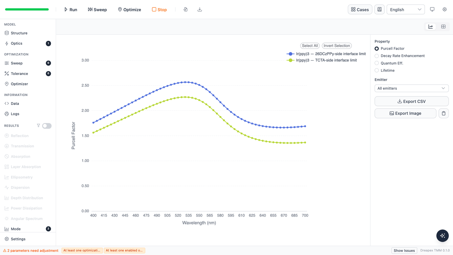
The raw software result is the same kind of curve. For the uncapped device, the two traces are the emitters on either side of the interface:
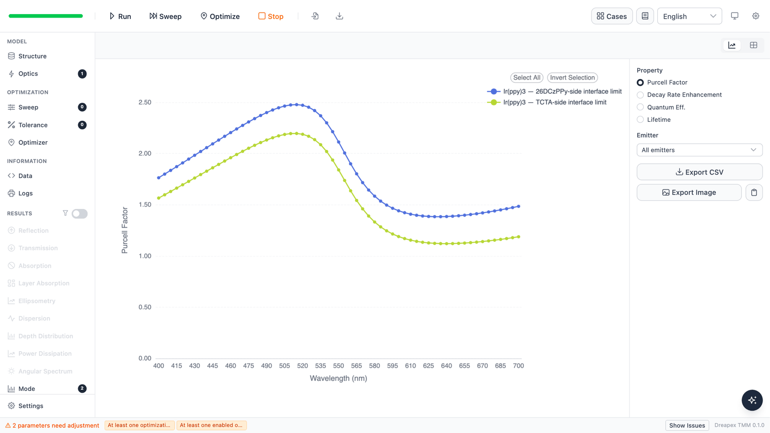
For the 90 nm device, both peak position and peak height recover with the capping layer:
Deviation Notes
Every layer uses a constant refractive index fixed at 520 nm, with no dispersion. Peak positions are therefore systematically red-shifted and the long-wavelength tail shape is only approximate; absolute values near 520 nm are unaffected.
The paper does not publish complex indices from the same batch, so this case uses open measurements of the same materials, deposited under different conditions and at different sample thicknesses than the paper's device; BmPyPB and 26DCzPPy additionally use optical proxies. The doped emissive sublayers reuse the optical constants of the undoped hosts, with no separate extinction term for the Ir(ppy)₃ concentration.
The paper fixes recombination at the interface between the two emissive sublayers but publishes neither the dipole orientation ratio nor which side an interfacial dipole belongs to. This case uses an isotropic source and the symmetric limit on both sides of the interface; a real recombination zone biased towards one layer would change the local optical environment and .