Outcoupling and Loss Split versus OLED Emitter Position
Light extraction and optical loss mechanisms in organic light-emitting diodes: Influence of the emitter quantum efficiency
Authors: Stefan Nowy, Benjamin C. Krummacher, Jörg Frischeisen, Nils A. Reinke, and Wolfgang Brütting
Journal: Journal of Applied Physics 104(12), 123109 (2008) · Comparison target: Figure 12
Move the recombination zone a few tens of nanometres between two organic layers of the same OLED stack and forward emission goes from just above 1% to 4.4%. The extra power does not disappear — it moves into the surface plasmon at the cathode and into the guided modes of the organic layers.
This case fixes the combined TPD and Alq3 thickness at 160 nm, walks the emission plane from the Ca cathode side to the ITO anode side over 29 runs, and reproduces the five power curves of paper Figure 12.
Direct emission peaks at nm with 4.40%, the sum of direct and substrate emission peaks further out at nm with 10.58%, and the plasmon channel falls monotonically from 49.7% at nm. Here is the Alq3 thickness, which is also the distance from the emission plane to the Ca cathode.
Background
The distance from the emission plane to the metal cathode decides where the energy goes. Too close, and the dipole couples straight into the cathode surface plasmon; at the right distance, more light escapes through the anode side. Nowy et al. fix the combined TPD and Alq3 thickness and change only how it is divided, so the emission plane moves while the total stack thickness stays put, and all six power curves fit on one chart.
The Mode result splits channels by the effective index that corresponds to the in-plane wavevector, matching the paper's curves one to one:
| Dreapex TMM channel | Effective-index range | Paper curve |
|---|---|---|
| Top Outcoupling | , crossing the glass–air interface | emission |
| Substrate | emission to substrate | |
| Waveguide | waveguiding | |
| Evanescent | plasmons | |
| Absorption | Power left in the propagating region that never crosses an outer boundary | absorption |
| Non-radiative | No wavevector range | all other |
and are the refractive indices of the glass substrate and the Alq3 layer. The six channels sum to the effective quantum efficiency, with the rest in the non-radiative channel. Moving the emission plane changes the Purcell factor, so every curve shifts at once.
Structure
The stack runs from the air incidence side to the Al cathode. TPD plus Alq3 always equals 160 nm; the scan changes both together.
| Given in the paper | Layer in the model | Thickness |
|---|---|---|
| Air | Incidence medium, | Semi-infinite |
| BK7 glass substrate (thickness not stated) | Glass substrate, incoherent | 1 mm |
| ITO anode | ITO | 140 nm |
| PEDOT:PSS | PEDOT:PSS | 30 nm |
| TPD hole-transport layer | TPD | nm |
| Alq3 emitting and electron-transport layer | Alq3, emissive | nm |
| Ca | Ca | 15 nm |
| Al cathode | Al | 100 nm |
Glass is the only incoherent layer and defines the substrate channel; it does not absorb, so its exact thickness does not matter. The 100 nm Al transmits essentially nothing, and bottom outcoupling measures 0.0000% in every run.
The paper publishes refractive indices only at 450 nm and 700 nm, with no full dispersion curve. The model uses published dispersion data for the same materials, resampled at 10 nm steps over 400–790 nm, with no scaling or shifting. At the two published endpoints:
| Material | Paper 450 nm → 700 nm | Used here | Difference |
|---|---|---|---|
| BK7 glass | 1.53 → 1.51 | 1.525 → 1.513 | ≤ 0.005 |
| ITO | 2.02 → 1.82 | 2.019 → 1.822 | ≤ 0.002 |
| PEDOT:PSS | 1.61 → 1.56 | 1.543 → 1.496 | −0.065 |
| TPD | 1.80 → 1.68 | 1.818 → 1.710 | ≤ 0.030 |
| Alq3 | 1.81 → 1.69, | 1.813 → 1.702, | ≤ 0.012 |
| Ca | 0.50 → 0.65; 1.69 → 2.79 | 0.587 → 0.680; 1.679 → 2.740 | |
| Al | 0.49 → 1.48; 4.60 → 6.98 | 0.488 → 1.481; 4.604 → 6.975 | ≤ 0.004 |
Six of the seven materials match at both endpoints to within 0.03. The one clear outlier is PEDOT:PSS, 0.065 low in , which is a formulation difference; that layer is only 30 nm thick, so the optical-path error is about 2 nm.
The structure page for the baseline device at nm. Only the TPD and Alq3 rows change during the scan, and the incoherent flag on the glass substrate must stay on:

Optical and Emitter Settings
The emitter sits in the Alq3 layer against the TPD side, with the paper's isotropic orientation and .
| Setting | Value | Basis |
|---|---|---|
| Emissive layer | Alq3 | The paper places an infinitely thin recombination zone at the TPD/Alq3 interface |
| Distribution and position | Delta, relative position 0.005 | A Delta emitter must lie strictly inside the layer, so the interface coordinate 0 is rejected; 0.005 puts the dipole 0.05 nm () to 0.75 nm () from the interface |
| Dipole orientation | Isotropic | The paper weights two parts parallel to one part perpendicular |
| Emission spectrum | Alq3 PL, 410–790 nm / 5 nm, peak 535 nm | Digitized independently from paper Figure 2 |
Spectrum Unit | Probability (channel fractions); Power (angle-resolved spectra) | The two settings differ by at most 0.19 percentage points across the six channels at nm |
| Quantum efficiency | 0.20 | Published value |
| Conversion efficiency / multiplier | 1 / 1 | Optical split only |
The three comparison figures share this one structure and differ only in the emission detector:
| Comparison target | Emission detector | Wavelength setting | Other settings |
|---|---|---|---|
| Figure 12 and the channel budget | Mode | Weighted Average, 420–780 nm, step 10 nm | — |
| Figure 7 angle-resolved spectra | Intensity | Sweep, 420–780 nm, step 2 nm | Angles 0–88°, step 2° |
| Figure 6 power-dissipation cross-section | Power Dissipation | Single, 525 nm | Effective index 0–3.5, step 0.002 |
The Mode detector settings used for the main comparison:

Each of the 29 positions in Figure 12 ( to 150 nm, step 5 nm) is a separate Run.
780 nm upper limit comes from the coverage of the TPD dispersion data (400–790 nm). The PL area outside the window is only 0.13% and does not affect the spectrally weighted result.Simulation Results and Comparison with Figure 12
Emitter-position scan
Paper Figure 12 is in the original article.
Paper readings (dashed) and the 29 runs (solid) on the same axes:
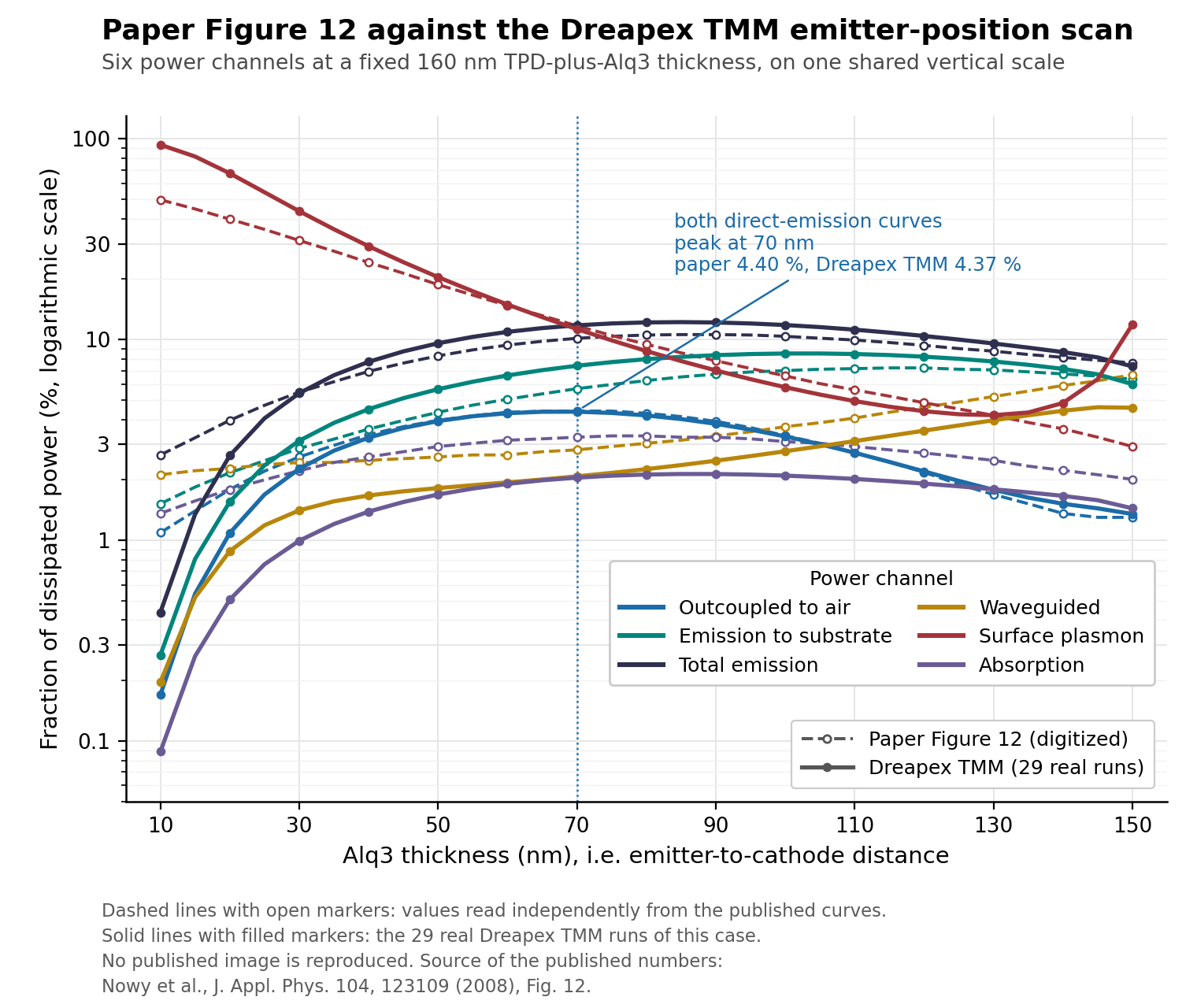
Three features can be checked digit by digit:
| Quantity | Paper | This run | Difference |
|---|---|---|---|
| Position of the direct-emission peak | 70 nm | 70 nm | 0 nm |
| Direct-emission peak value | 4.40% | 4.37% | 0.03 percentage points |
| Position of the direct-plus-substrate peak | 85 nm | 85 nm | 0 nm |
Point-by-point absolute differences per channel, in percentage points:
| Window and statistic | Emission | Substrate | Emission + substrate | Waveguide | Plasmon | Absorption |
|---|---|---|---|---|---|---|
30–140 nm maximum | 0.33 | 1.75 | 1.65 | 1.48 | 12.44 | 1.24 |
30–140 nm RMS | 0.11 | 1.30 | 1.26 | 0.95 | 3.36 | 1.06 |
10–150 nm maximum | 0.92 | 1.75 | 2.22 | 2.11 | 43.69 | 1.31 |
The emission, substrate, and waveguide curves track point by point across the whole window. The large plasmon differences sit at the end where the emission plane approaches the metal; see below.
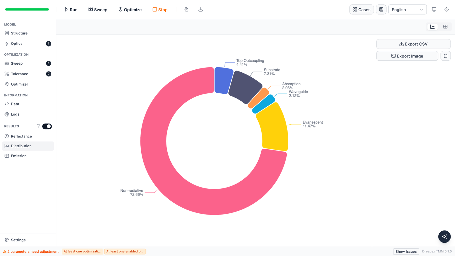
The Mode result at the peak position, with 4.368% top outcoupling, 7.400% substrate, and a Purcell factor of 1.492:
Channel budget of the baseline device
The paper publishes a six-channel budget for the baseline device at nm. The run at the same position:
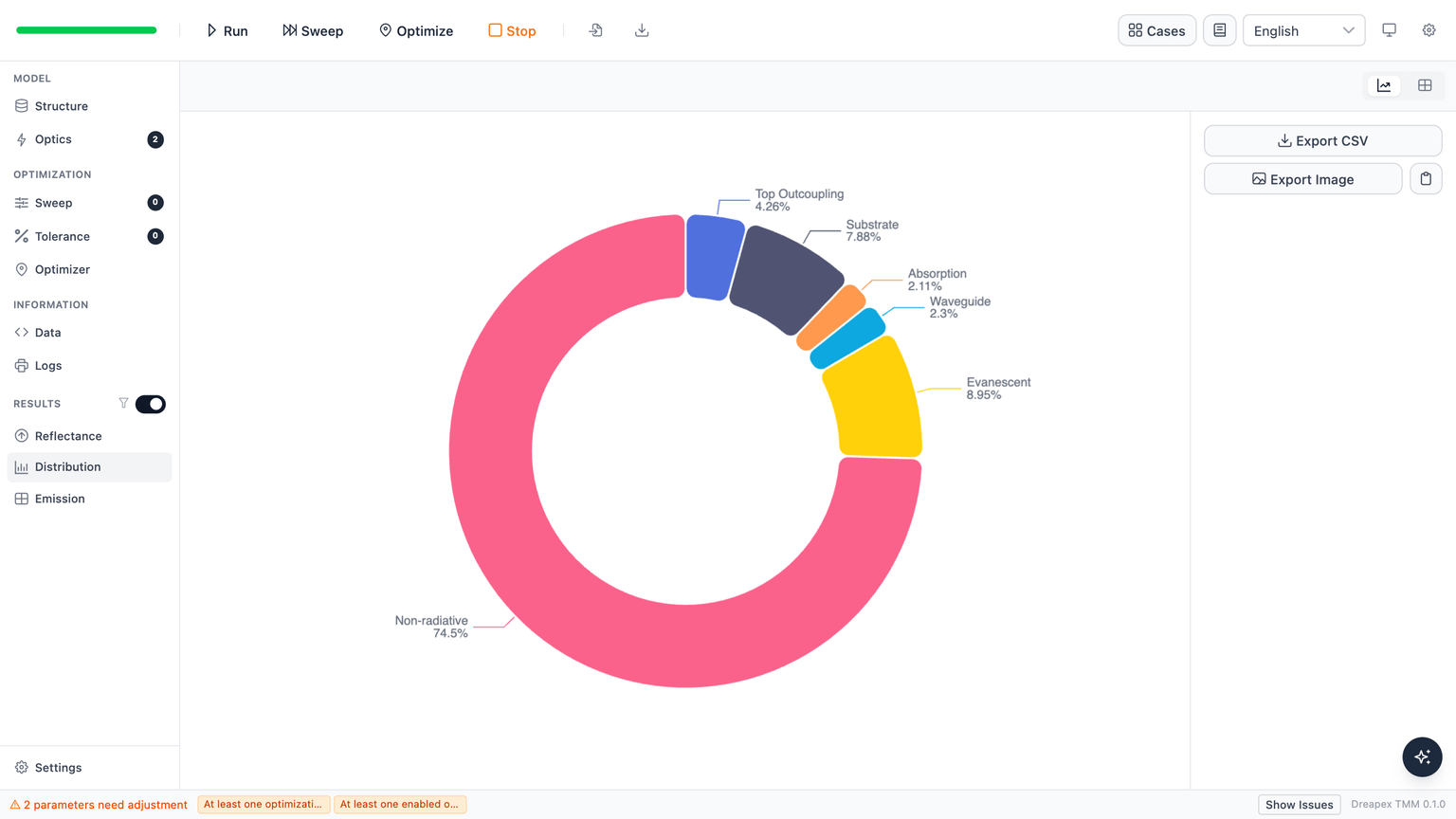
| Channel | Paper | This run | Difference |
|---|---|---|---|
| Top outcoupling | 4.2% | 4.19% | −0.01 percentage points |
| Substrate | 6.3% | 7.98% | +1.68 percentage points |
| Waveguide | 3.0% | 2.26% | −0.74 percentage points |
| Evanescent (plasmon) | 9.5% | 8.76% | −0.74 percentage points |
| Absorption | 3.3% | 2.13% | −1.17 percentage points |
| Non-radiative | 73.6% | 74.69% | +1.09 percentage points |
The largest difference, 1.68 percentage points, is in the substrate channel; top outcoupling matches almost digit for digit. This run has a Purcell factor of 1.356 and an effective quantum efficiency of 0.2531, which with the 0.7469 non-radiative channel sums to 1.0000.
10 nm should be 64.08; this run gives 63.53 and the paper curve implies 5.04. Real devices operate far from this range.Mode positions and polarization
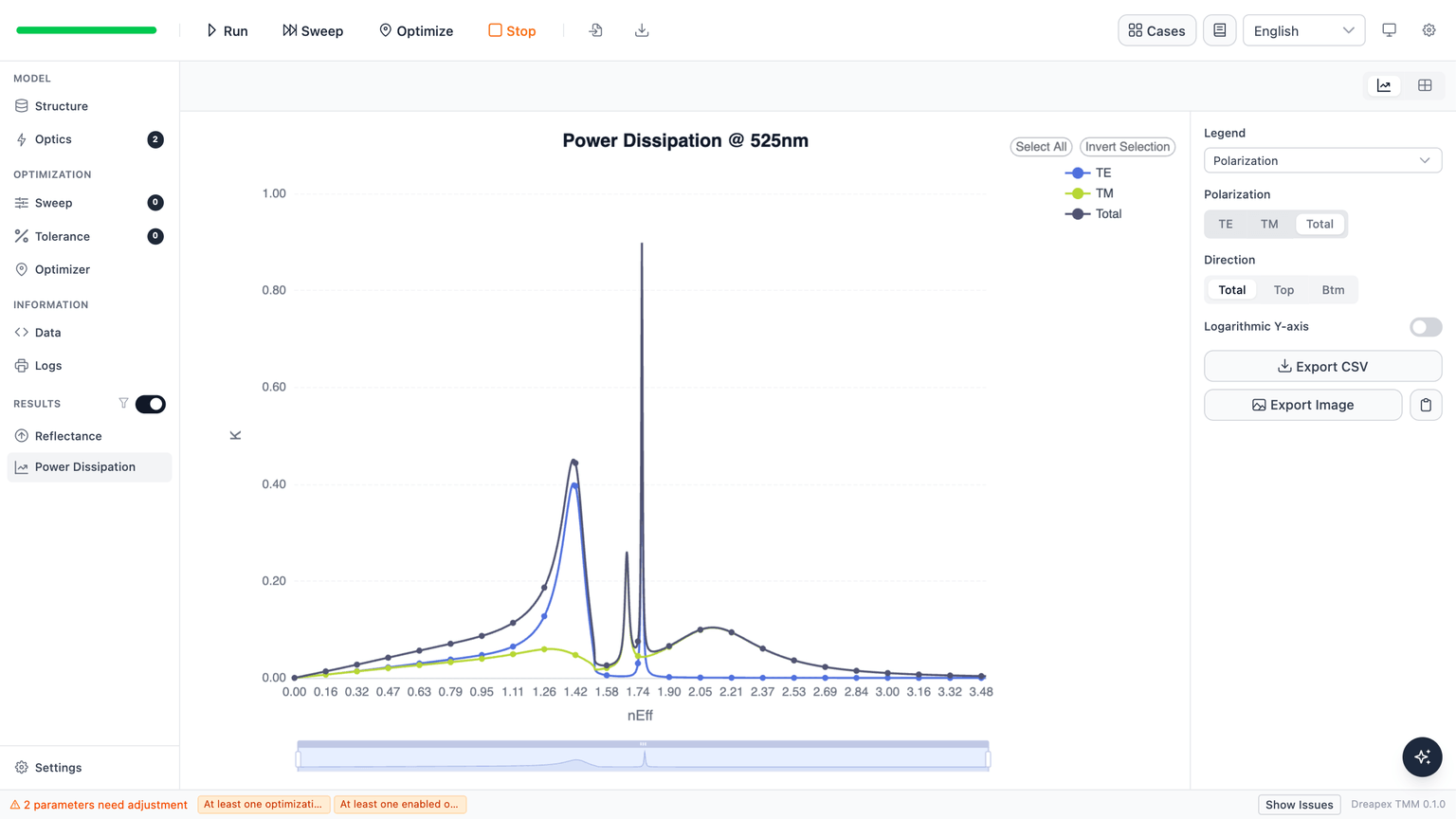
The channel split depends on where each mode sits on the effective-index axis, and paper Figure 6 gives a 525 nm power-dissipation cross-section for checking them one by one. Switch the detector to Power Dissipation:

The resulting cross-section shows the substrate region, two device waveguide modes, and the surface plasmon in order:
| Feature | Paper | This run | Difference | Polarization here | Paper's identification |
|---|---|---|---|---|---|
| Substrate-region maximum | 1.404 | 1.412 | +0.008 | TE | Matches; the paper calls the substrate mode TE |
| Device waveguide mode 1 | 1.688 | 1.682 | −0.006 | TM | Matches |
| Device waveguide mode 2 | 1.755 | 1.758 | +0.003 | TE | Matches |
| Surface plasmon | 2.106 | 2.116 | +0.010 | TM | Matches; the paper calls the SPP always TM |
All four mode positions agree to within 0.010, and all four polarization assignments match. Peak heights are not compared: the displayed height of a sharp guided-mode resonance depends on the wavevector sampling step.
Angle-resolved emission spectra
Paper Figure 7 gives s- and p-polarized angle-resolved emission spectra for this device. Switch the detector to Intensity and set the wavelength and angle ranges:

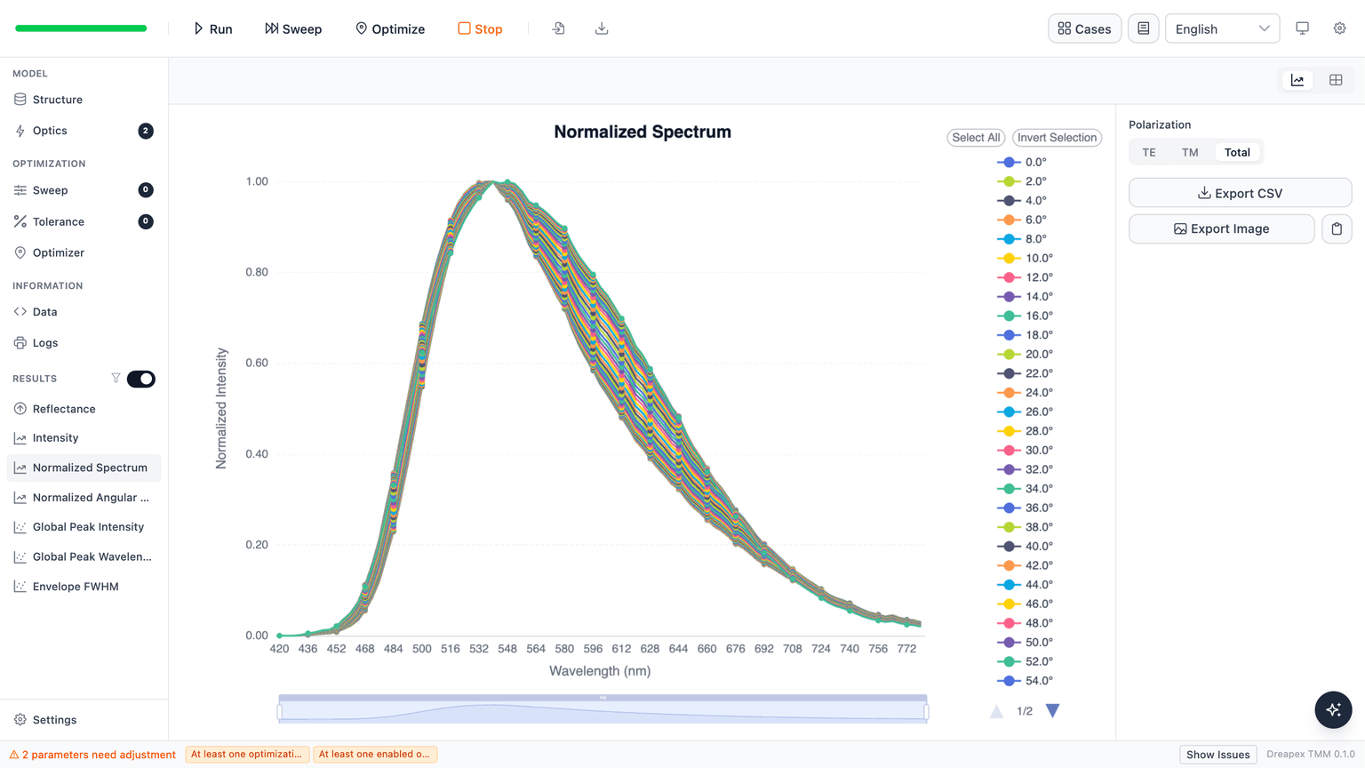
Normalized emission spectra versus angle, where the s-polarized band centre shifts clearly to the red:
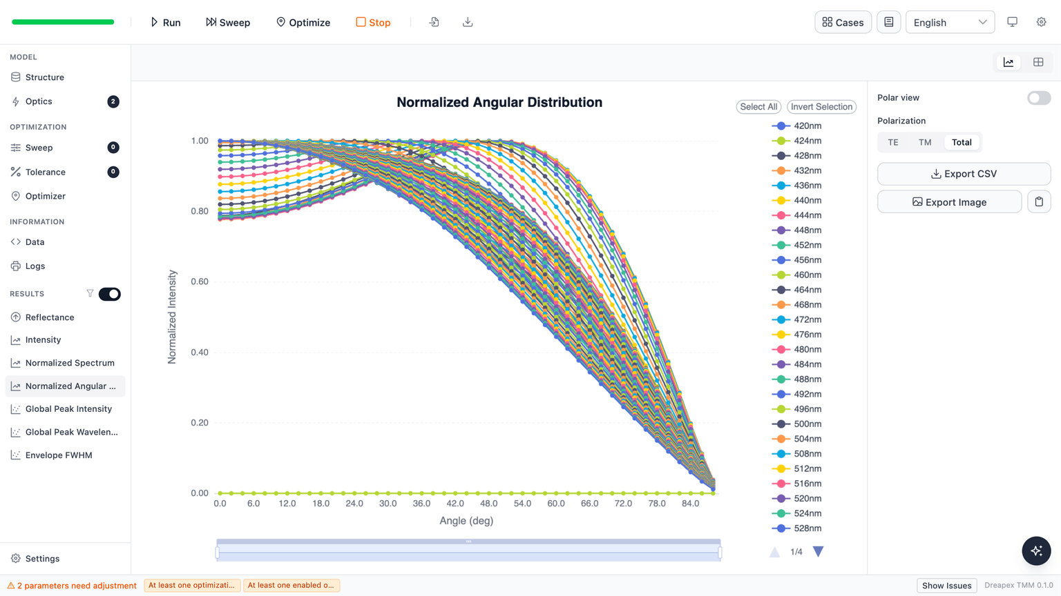
The spectrally integrated angular distribution, each polarization normalized to 0°:
| Quantity | Polarization | Maximum difference | RMS difference |
|---|---|---|---|
| Band centre (0–80°) | s | 2.8 nm | 2.3 nm |
| Band centre (0–80°) | p | 2.9 nm | 2.0 nm |
| Normalized angular distribution | s | 4.78% (at 80°) | 1.54% |
| Normalized angular distribution | p | 2.24% (at 50°) | 1.32% |
The trend of the band centre is reproduced as well: the paper's s polarization shifts from 556 nm at 0° to 570 nm at 80°, this run gives 553 → 572 nm; for p the paper gives 555 → 558 nm and this run 553 → 557 nm. That s/p asymmetry is the origin of the colour stability the paper highlights.
Deviation Notes
The paper publishes refractive indices only at two endpoints, so the substitute dispersion data in the table are assumed inputs. PEDOT:PSS runs 0.065 low in , which shifts the cavity phase slightly.
The paper's emission plane is an ideal infinitely thin sheet. The model approximates it with a Delta emitter at a relative position of 0.005, which shortens the dipole-to-cathode distance systematically by 0.05 to 0.75 nm.
is the paper's input value and is used as published; absolute outcoupling efficiency scales linearly with it. The comparison is against the paper's calculated curves, not its measured ones.