Emission Position and Outcoupling Efficiency in a Broad-Recombination OLED
Optical Outcoupling Efficiency of Organic Light-Emitting Diodes with a Broad Recombination Profile
Authors: Yungui Li, Naresh B. Kotadiya, Bas van der Zee, Paul W. M. Blom, Gert-Jan A. H. Wetzelaer
Journal: Advanced Optical Materials 9, 2001812 (2021) · Comparison target: Figure 2 and Figure 3c
Move the emission plane from the cathode side toward the anode side and the outcoupling efficiency first rises and then falls, with the maximum occupying only a short stretch of the emissive layer. A real single-layer device has no such plane — its recombination zone spreads over tens of nanometres and sits on a whole segment of that curve at once.
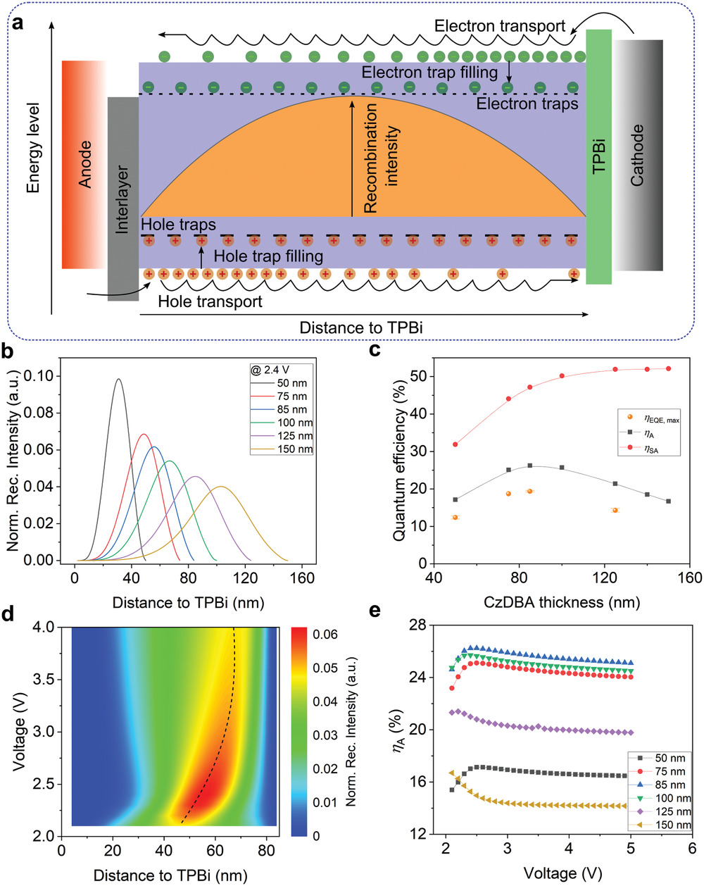
This case first scans the delta emission-plane position to reproduce the twelve curves of paper Figure 2, then weights them with the paper's recombination profile to get the optimum emissive-layer thickness of Figure 3c.
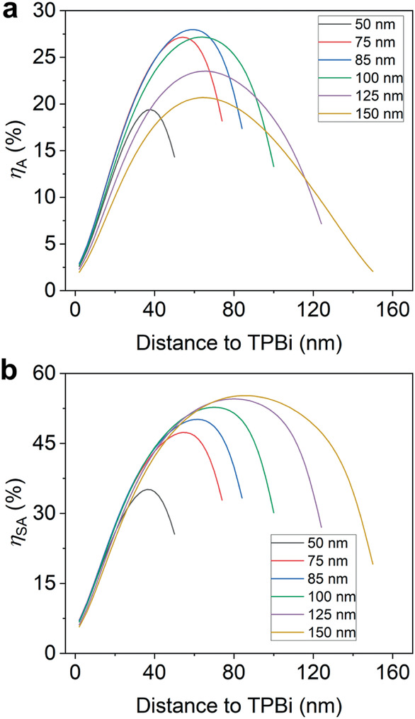
The maxima of the six curves move toward the anode side as the emissive layer thickens, and become very flat at 125 and 150 nm. The four digitized peaks each land within 0.05 percentage points of the 19.4 %, 28.0 %, 35.1 %, and 55.2 % stated in the paper text.
Background
In a bottom-emitting device, the power that escapes to air through the glass surface is ; adding the share trapped by total internal reflection in the glass substrate, which can only leave through the substrate edge, gives . The paper seals the substrate edges with the sample holder so substrate modes are not collected, which matches this split.
The outcoupling efficiency of a single delta emission plane depends only on its position inside the emissive layer — the distance to the CzDBA/TPBi interface, with on the cathode side. Scanning point by point produces the curves of paper Figure 2. In a real device excitons are generated along a recombination profile, so the outcoupling efficiency is the average of that curve weighted by the profile.
Structure
The stack is built from the glass substrate side. All seven layer thicknesses take their published values, with no registration. The 560 nm optical inputs below are the interpolated values actually used.
| Layer | Thickness | Optical input at 560 nm | Thickness source |
|---|---|---|---|
| Glass substrate | 1 mm, incoherent | , | Not stated in the paper; assumed here |
| ITO anode | 120 nm | , | Given in the paper |
| PEDOT:PSS hole-injection layer | 40 nm | , | Given in the paper |
| MoO₃ hole-injection layer | 6 nm | , | Given in the paper |
| C60 interlayer | 3 nm | , | Given in the paper |
| CzDBA emissive layer | 50 / 75 / 85 / 100 / 125 / 150 nm | , | Given in the paper |
| TPBi electron-transport layer | 4 nm | , | Given in the paper |
| Al cathode | 100 nm | , | Given in the paper |
1.90 at 380 nm and 1.65 at 900 nm; every other layer uses the matching entry in the built-in material database. This is the largest input uncertainty in the case.The 85 nm variant once entered. The first row shows glass in mm and flagged incoherent, and the emissive marker on the CzDBA row indicates the Delta emitter in that layer:

The six models differ only in CzDBA thickness; every other layer and thickness is identical.
Optical and Emitter Settings
| Setting | Value | Source |
|---|---|---|
| Emitter count and distribution | One Delta emission plane | The modelling approach of paper Figure 2 |
| Anisotropy factor | Vertical dipole fraction 0.148 | Fitted by the paper from neat-film angle-resolved photoluminescence |
| Emitter position | Sweep 0.01 to 0.99, step 0.01, 98 points per thickness | The paper's independent variable |
| Emission spectrum | Peak 560 nm, FWHM 84 nm | The paper gives no intrinsic spectrum; the average of three device electroluminescence spectra is used |
| Spectrum Unit | Probability | Matches the photon-count weighting of Mode |
| Quantum efficiency, conversion efficiency, multiplier | All 1 | Matches the paper's purely optical convention |
| Detectors | Emission Mode + Propagation R | A run requires at least one base detector; the R result is not used in the comparison |
| Wavelength mode | Weighted Average, 450–780 nm, step 5 nm | — |
The Top Outcoupling channel of Mode is ; adding the Substrate channel gives .

The emitter position is measured from the C60 interface on the anode side, and the paper's horizontal axis follows , where is the relative position in the emissive layer and its thickness. For the 85 nm device, p = 0.30 corresponds to . Scanning all six thicknesses gives 588 position points.
Sweep for the emission-plane position, not Optimize. The optimum emissive-layer thickness is fitted from the six weighted results.Simulation Results and Comparison with Figure 2 and Figure 3c
Emission-plane position curves
Paper Figure 2 is in the original article.
The same six thicknesses and the same two quantities, with the scan results (solid) overlaid on the extracted paper values (markers):
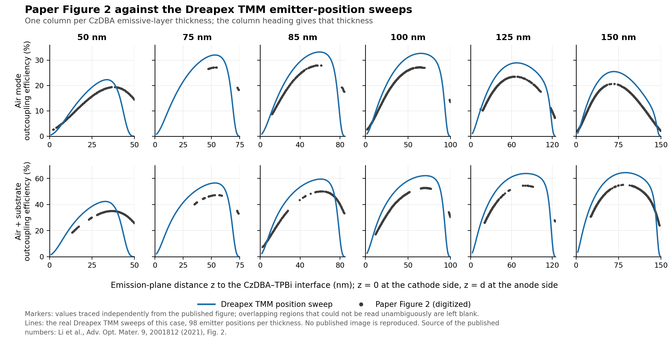
The extremum position is located by a parabolic fit over the top 3 % of each curve, so digitization noise on a flat top does not dominate.
| Quantity | Emissive-layer thickness | This run | Paper | Difference |
|---|---|---|---|---|
50 nm | 33.5 nm | 37.6 nm | −4.0 nm | |
75 nm | 52.6 nm | 54.0 nm | −1.3 nm | |
85 nm | 58.9 nm | 59.4 nm | −0.5 nm | |
100 nm | 65.1 nm | 63.6 nm | +1.5 nm | |
125 nm | 68.0 nm | 65.5 nm | +2.4 nm | |
150 nm | 67.1 nm | 65.0 nm | +2.2 nm | |
50 nm | 32.6 nm | 36.7 nm | −4.1 nm | |
75 nm | 52.4 nm | 54.7 nm | −2.3 nm | |
85 nm | 59.7 nm | 61.1 nm | −1.5 nm | |
100 nm | 69.6 nm | 70.0 nm | −0.4 nm | |
125 nm | 81.1 nm | 80.2 nm | +1.0 nm | |
150 nm | 87.7 nm | 85.9 nm | +1.8 nm |
Across the twelve curves the maximum difference is 4.1 nm, the RMS difference 2.2 nm, and the mean difference −0.4 nm. The maxima themselves are flat: the plateau above 99 % of peak spans 3.5 to 22.5 nm here and 4.3 to 19.3 nm in the paper. Normalizing each curve to its own peak and comparing point by point gives a mean RMS difference of 3.29 % of peak.
Three positions from the same scan, read on the Mode result. At the optimum, , 33.19 % escapes to air and 26.28 % stays in the substrate, with a Purcell factor of 1.32:

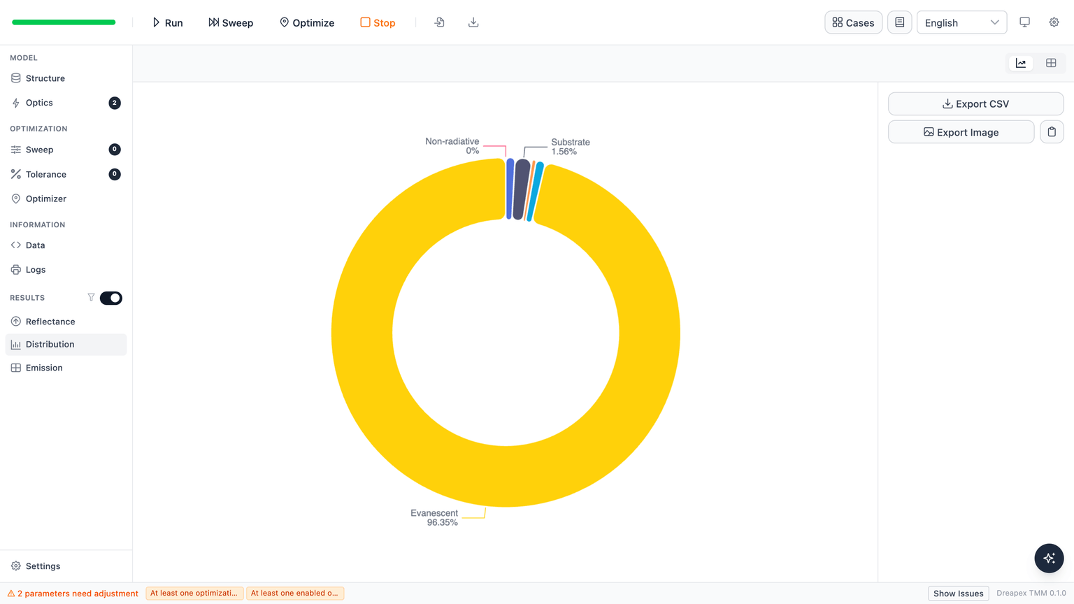
Pressed against the cathode-side interface (), the air mode drops to 0.85 %, 96.35 % goes evanescent, and the Purcell factor rises to 8.71:
Pressed against the C60 interface (), the air mode collapses to 0.04 % and the Purcell factor reaches 1264.89:
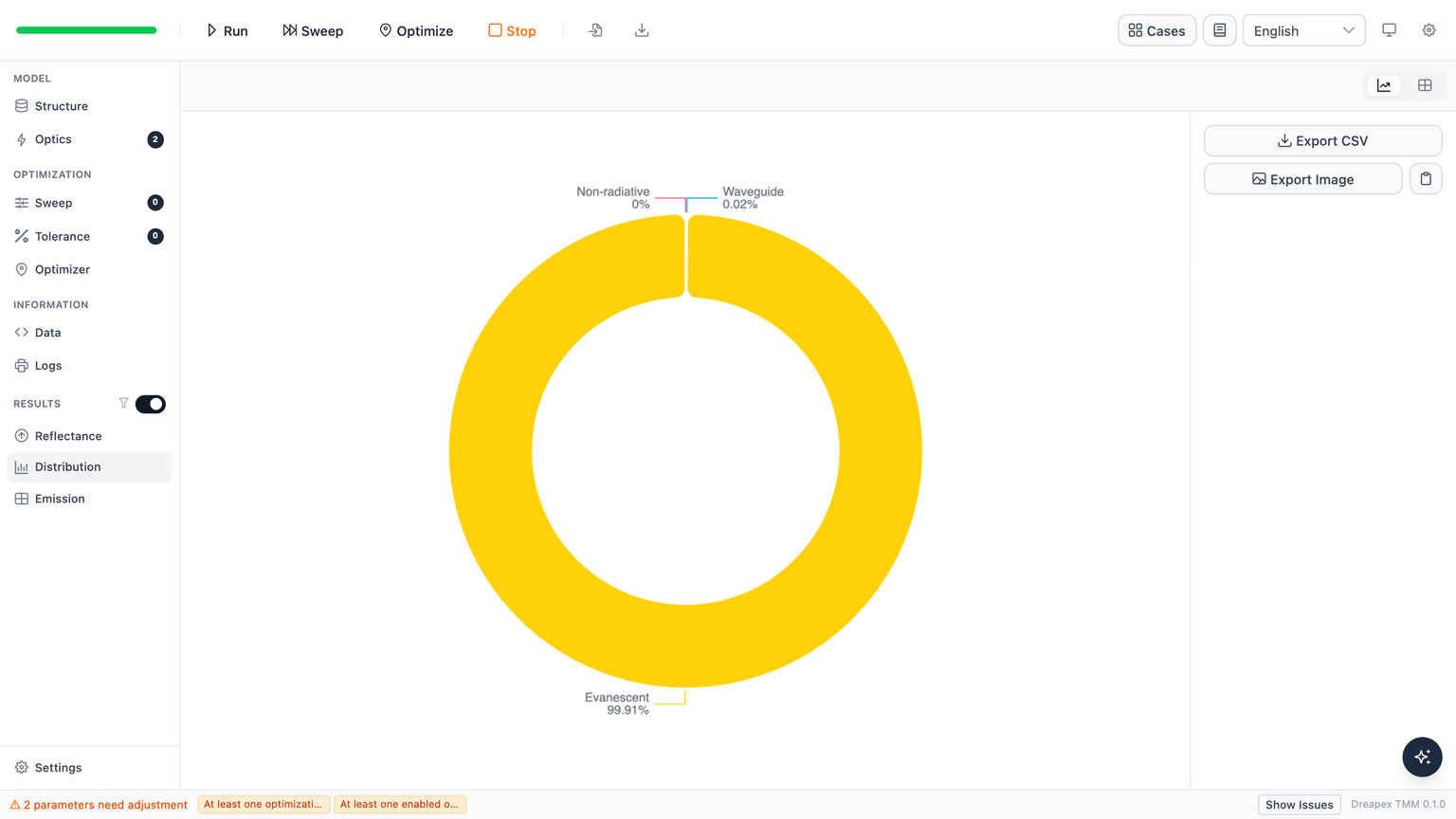
The paper's curve does not collapse at the same position; the extracted value is still 17.5 %. Replacing C60 with a lossless layer of the same refractive index brings this run back to 23.54 %, which places the difference in the C60 extinction coefficient. It affects only the last 10 nm next to the anode interface.
Recombination-weighted optimum thickness
Weighting each thickness's position curve with the paper's recombination profile collapses the twelve curves into two curves versus thickness, which is what paper Figure 3c reports (see the original article).
The same quantities on one set of axes:
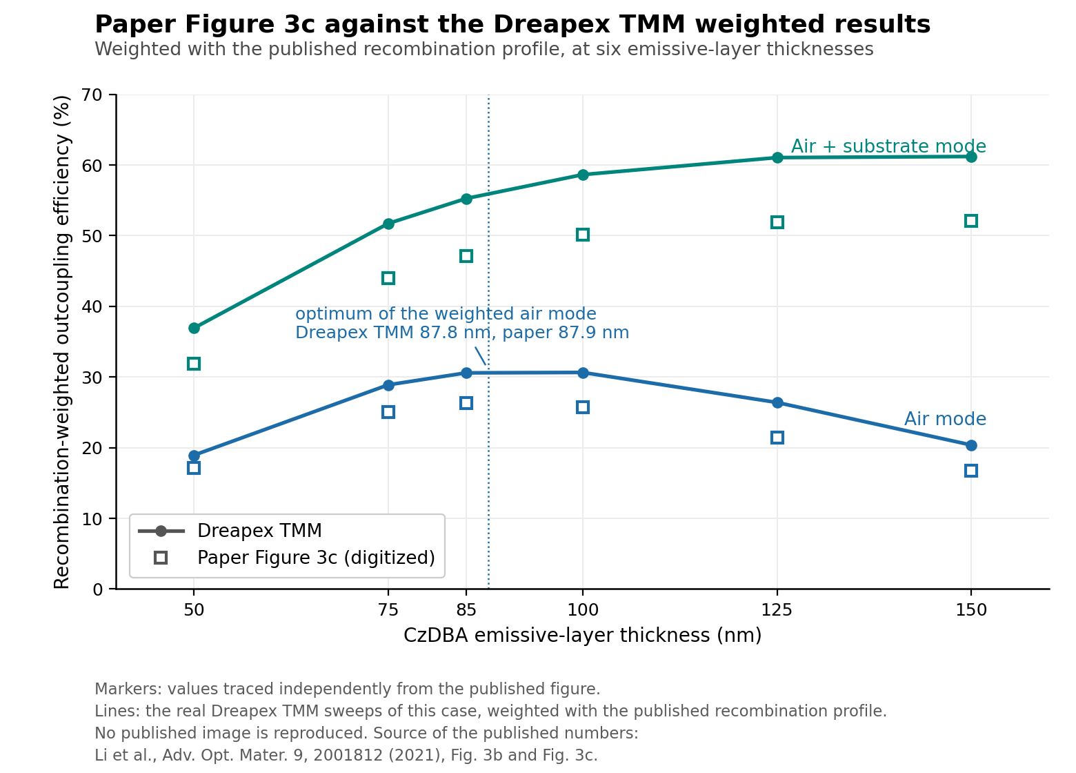
| Emissive-layer thickness | Weighted here | Paper | Difference | Weighted here | Paper | Difference |
|---|---|---|---|---|---|---|
50 nm | 18.94 % | 17.15 % | +1.79 | 36.93 % | 31.92 % | +5.01 |
75 nm | 28.89 % | 25.04 % | +3.85 | 51.73 % | 44.03 % | +7.70 |
85 nm | 30.59 % | 26.28 % | +4.31 | 55.25 % | 47.14 % | +8.11 |
100 nm | 30.64 % | 25.73 % | +4.91 | 58.63 % | 50.16 % | +8.47 |
125 nm | 26.40 % | 21.42 % | +4.98 | 61.05 % | 51.91 % | +9.14 |
150 nm | 20.37 % | 16.71 % | +3.66 | 61.20 % | 52.12 % | +9.08 |
Differences are in percentage points. The optimum emissive-layer thickness, located by a parabola vertex, is 87.8 nm here against 87.9 nm in the paper, a difference of 0.1 nm. A single common scale factor of 0.848 brings the whole thickness curve onto the paper's, with an RMS difference of 0.70 percentage points over the six points.
The cost of broadening is the gap between the delta-plane optimum and the weighted value: for the 85 nm device it is 2.60 percentage points here, a relative loss of 7.8 %, against 1.70 points and 6.1 % in the paper. Spreading the recombination zone from a plane across the whole layer costs about two percentage points of outcoupling efficiency.
Deviation Notes
The CzDBA refractive index is the one published input that could not be obtained, and the largest source of uncertainty. Replacing it with a constant shifts the maxima by 0 to −3.8 nm and moves the optimum-thickness vertex from 87.8 nm to 83.7 nm, the same order as the 4.1 nm largest residual of the main comparison.
Absolute outcoupling efficiency runs 15 % to 23 % above the paper, which points at two other assumed inputs: the ITO dataset has an extinction coefficient of exactly zero across the visible and so underestimates anode absorption, and a low CzDBA index widens the escape cone into air. Orientation is not a cause — 0.148 is taken directly from the paper.
The reference values come from independent digitization of the published figures, not from numerical source data.