Bidirectional Vertical Radiance Ratio of a Transparent Perovskite LED
Transparent Perovskite Light-Emitting Diodes with Conductive Oxide Top Electrodes
Authors: Michele Forzatti, Sergio Martínez-Saiz, Morena Cervino, Edoardo Stanzani, Sandra Jenatsch, Qingsen Zeng, Joo Sung Kim, Dong-Hyeok Kim, Eojin Yoon, Tae-Woo Lee, Daniel Tordera, and Henk J. Bolink
Journal: Advanced Materials e21688 (2026) · Comparison target: Figure S11
Once a light-emitting device is transparent on both faces, the brightness seen through the glass and the brightness seen through the top electrode are not equal, even though both directions share the same excitons. The whole difference is optical: the layer stacks on the two sides of the emission point are different, so the interference conditions for escaping light are different.
This case computes the same stack forwards once and reversed once, divides the two 0° radiance spectra to get the bottom-to-top ratio of paper Figure S11, and reproduces its dependence on both electrode thicknesses with one two-dimensional sweep.
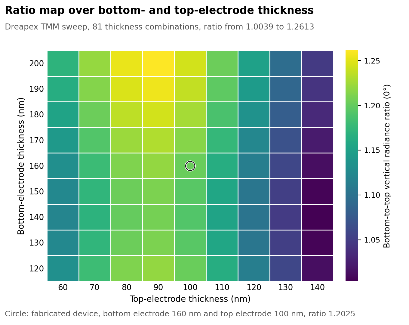
The ratio stays above 1.00 across the whole thickness window, so the bottom face is always the brighter one. The red point is the fabricated device (bottom electrode 160 nm, top electrode 100 nm), labelled 1.18.
Background
Both electrodes of this device are transparent conducting oxides with no metal mirror, and air is the exit medium on both sides. The same pixel therefore emits in both directions: at 6.0 V the paper measures more than 80 000 cd m⁻² from the bottom face and 68 000 cd m⁻² from the top.
The two directions differ only in their outcoupling factors — injected current, internal quantum efficiency, and the emitter's intrinsic spectrum all cancel in the ratio. The ratio therefore tests the optical model on its own, without knowing the device's electrical performance or emission efficiency, and without calibrating absolute output.
Structure
The stack runs from the glass substrate side. The 538 nm optical inputs are the interpolated values actually used.
| Layer | Thickness | Optical input at 538 nm |
|---|---|---|
| Glass substrate | 1.1 mm | , , treated as incoherent |
| ITO bottom electrode | 160 nm | , |
| Perovskite emissive layer | 150 nm | , |
| PO-T2T electron-transport layer | 20 nm | T2T proxy, , |
| SnOx buffer layer | 20 nm | , (assumed) |
| ITO top electrode | 100 nm | Same dataset as the bottom electrode, , |
All thicknesses come from the paper and are confirmed by its cross-sectional electron micrograph. The emissive-layer and glass are stated directly in the paper. ITO uses a published measured dataset for commercial sputtered ITO; the top electrode is pulsed-laser deposited and has no dedicated measurement, so the same dataset stands in. PO-T2T is proxied by the ordinary index of T2T, a triazine of the same family. The buffer layer takes , , based on the published 1.78–1.95 range for atomic-layer-deposited SnO₂.
The bottom-face direction uses the forward stack, with 1.1 mm glass flagged incoherent in the first row and the emissive marker on the perovskite layer:

The top-face direction reverses the whole stack: the first row becomes the 100 nm top electrode and glass moves to the end, with no change in thickness or material:

Intensity reports the far field emitted toward the top medium, so the two directions require two runs. The reversal introduces no unphysical difference: on a strictly symmetric stack, forward and reversed Intensity outputs are identical at all 131 wavelength points.Optical and Emitter Settings
Both directions share the same emitter and detector settings.
| Setting | Value |
|---|---|
| Recombination profile | Gauss, peak at the centre of the emissive layer (relative position 0.5), width 50 nm, 51 sample points |
| Dipole orientation | Isotropic |
| Emission spectrum | Gaussian, peak 538 nm, FWHM 22 nm, covering 380–800 nm |
| Spectrum Unit | Probability |
| Quantum efficiency, conversion efficiency, multiplier | All 1 (they cancel in the ratio) |
| Detectors | Emission Intensity and Mode; Propagation R, T, A |
| Emission wavelength sampling | Sweep, 480–610 nm, step 1 nm |
| Emission angle | Single, 0° |
The profile shape, peak position, and width are all fixed by the paper and entered as published. The Gauss Width field is a standard deviation, so 50 nm goes in directly.

The thickness map is generated with Sweep: bottom electrode 120–200 nm and top electrode 60–140 nm, both in 10 nm steps, 81 combinations each for the forward and reversed stack.
Run for individual device spectra and Sweep for the two-dimensional thickness map. It does not use Optimize.Simulation Results and Comparison with Figure S11
Ratio at the fabricated thicknesses
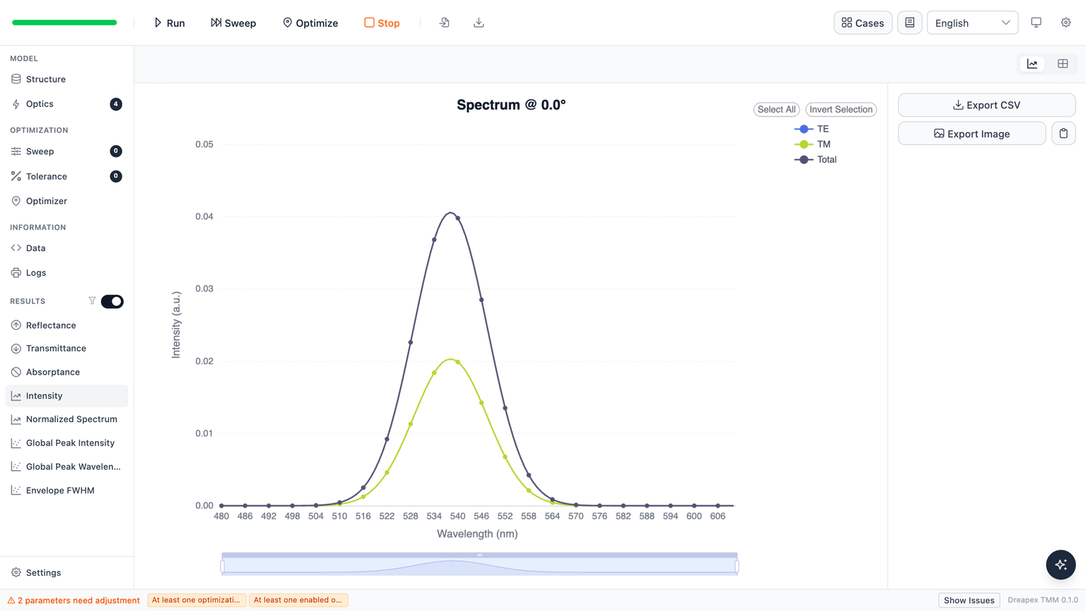
The 0° radiance spectrum for the bottom face, peaking at 0.04058:
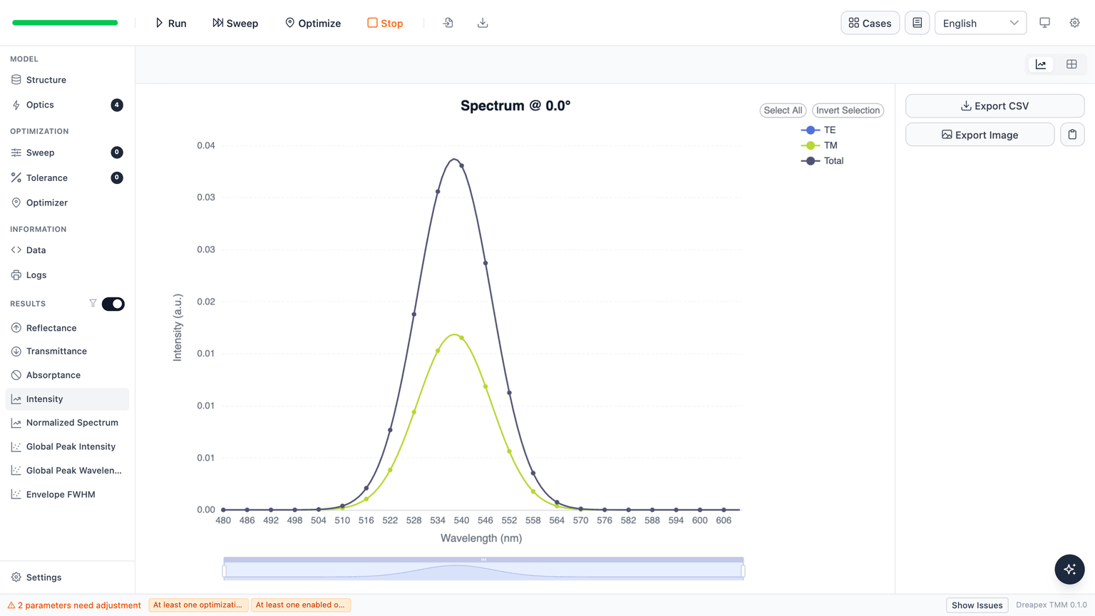
The top-face spectrum from the reversed stack, peaking at 538 nm as well with a value of 0.03372:
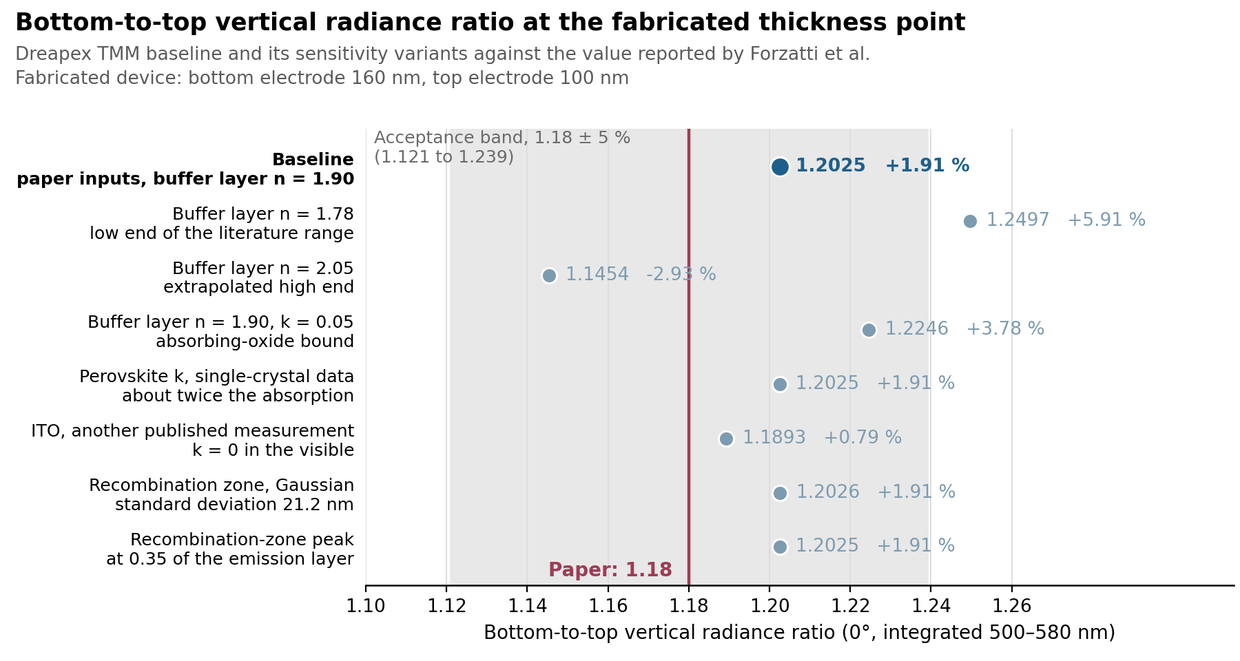
Integrating both over 500–580 nm and dividing gives 1.2025, which is +1.91% from the paper's 1.18, with no fitting parameters used.
Two-electrode thickness map
Paper Figure S11 appears in the Supporting Information of the original article.
Dividing the forward and reversed sweeps gives the same quantity as paper Figure S11, with the axes swapped and the same coverage:
| Quantity | Paper | Dreapex TMM |
|---|---|---|
| Ratio at the fabricated thicknesses | 1.18 | 1.2025 (+1.91%) |
| Range of the map | 1.00–1.25 | 1.0039–1.2613 |
| Top-electrode thickness at the maximum | Ridge in the figure | 90 nm, identical on all 9 rows |
| Bottom-electrode thickness at the minimum | Valley in the figure | 140 nm, identical on all 9 columns |
Across 81 thickness combinations the ratio spans 1.0039–1.2613, essentially coincident with the paper's 1.00–1.25 colour scale.
Wavelength dependence of the ratio
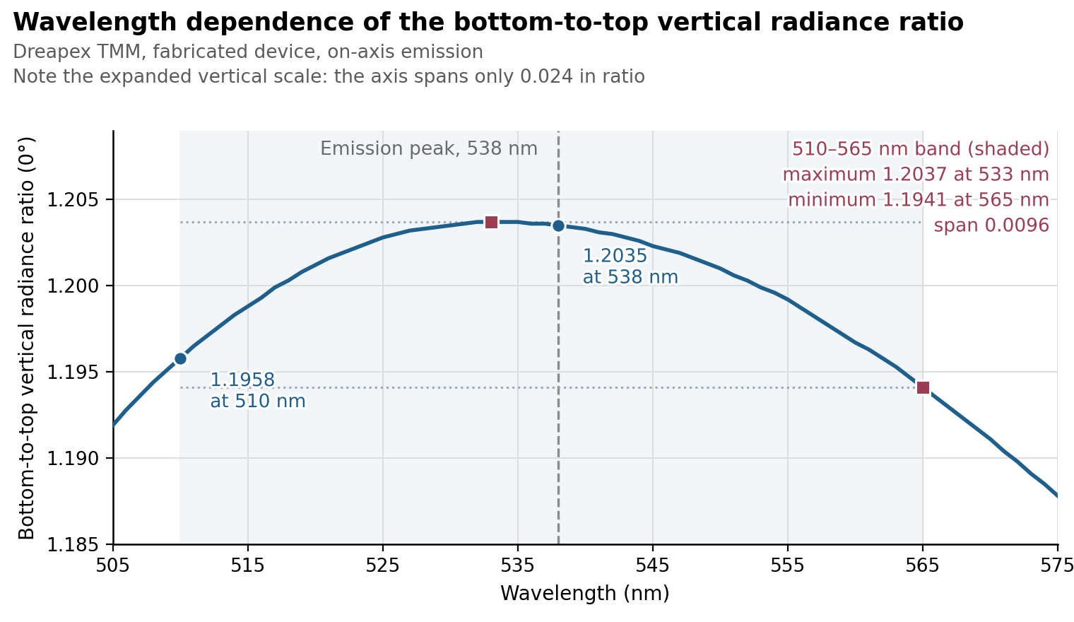
The ratio is nearly constant across the emission band: 1.1958 at 510 nm, 1.2035 at 538 nm, and a total span of only 0.0096 over 510–565 nm. The cavity effect is weak, so the two emitted lineshapes are essentially the same — an independent reproduction of the paper's observation that the normalized electroluminescence spectra of the two directions overlap.
Mode fractions
Switching the same model to the Mode detector shows where this 11.4% of double-sided outcoupling sits in the total power:
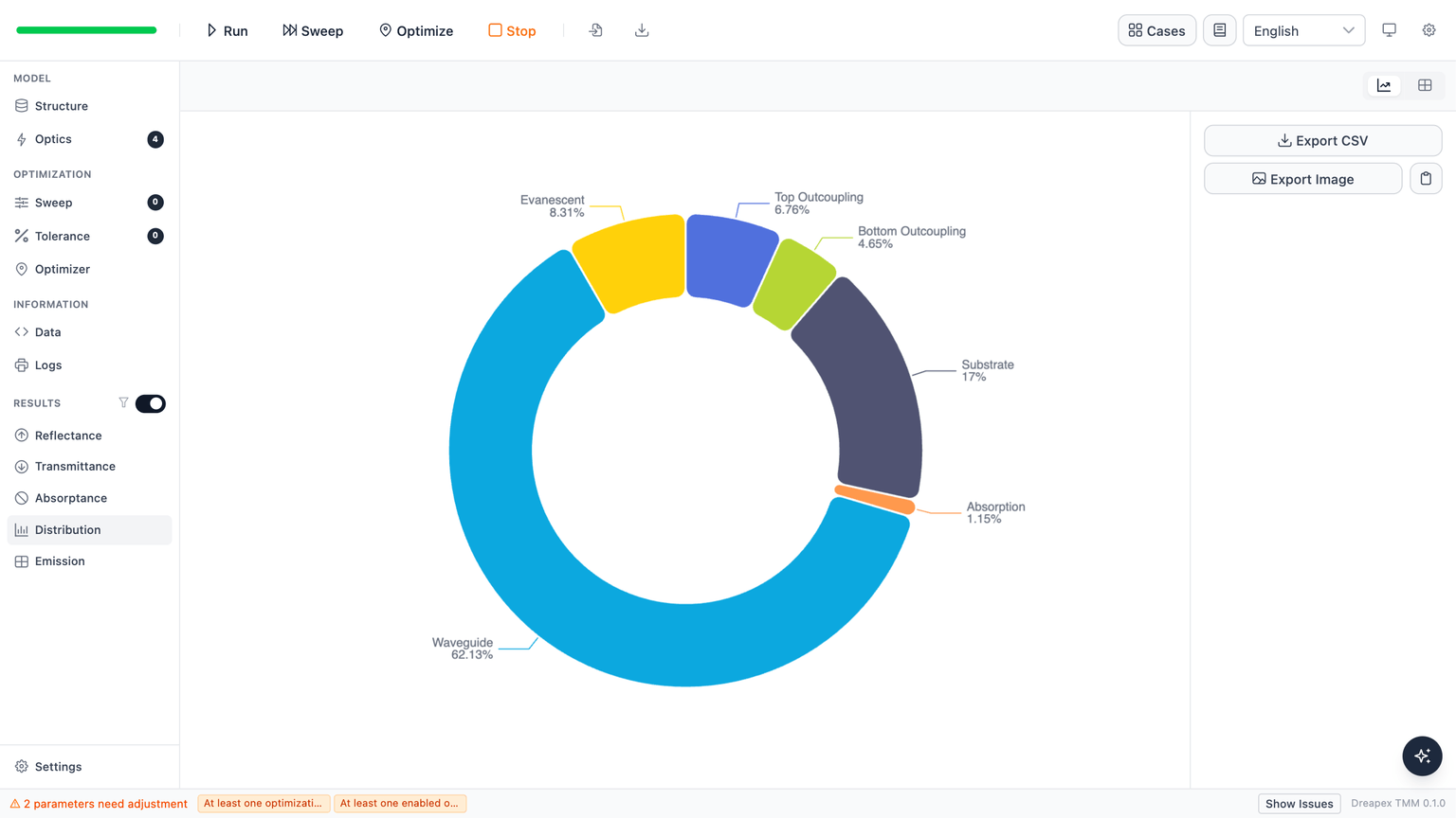
| Channel | Fraction |
|---|---|
| Top outcoupling (bottom face, through the glass) | 6.76% |
| Bottom outcoupling (top face, through the top electrode) | 4.65% |
| Substrate | 17.00% |
| Waveguide | 62.13% |
| Evanescent | 8.31% |
| Absorption | 1.16% |
The Purcell factor is 1.044. The mode fractions give a total-flux ratio of 1.4545, larger than the on-axis radiance ratio of 1.2025 because the angular distribution on the glass side is broader. Both of the paper's anchors are on-axis quantities, so the main comparison uses the 0° output of Intensity.
Deviation Notes
The buffer-layer is the one input with no published source, and the single material parameter the ratio is most sensitive to: sweeping it over 1.78–2.05 puts the ratio between 1.1454 and 1.2497, bracketing the paper's 1.18. The top electrode uses sputtered ITO data in place of the pulsed-laser-deposited film; another published dataset gives 1.1893, about 1% different.
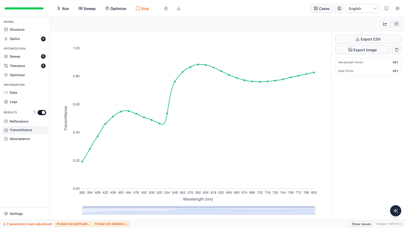
As an independent structural check, the transmittance spectrum of the same model against the three measured anchors of paper Figure 2g:
Overlaying that curve on the three measured anchors:
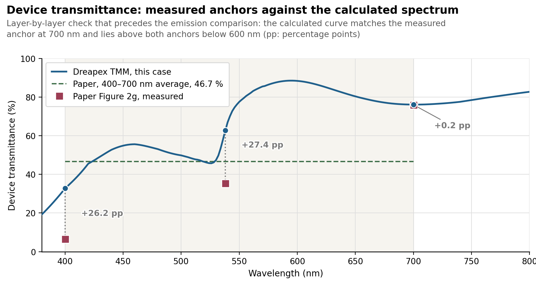
At 700 nm the two agree to 0.2 percentage points (75.9% against 76.11%), which confirms the layer thicknesses, layer order, and ITO index. Below 600 nm the gap grows toward the blue, reaching 27.4 percentage points at 538 nm, because the extinction-coefficient source the paper cites peaks at 0.133, roughly half the published single-crystal value, and because a one-dimensional planar model contains no thin-film scattering. This is decoupled from the ratio comparison: replacing the emissive-layer extinction with a dataset absorbing about twice as strongly leaves Intensity identical at all 131 wavelength points.
The emission spectrum uses a Gaussian in place of the measured photoluminescence curve, which was not obtained; since the ratio only varies between 1.1941 and 1.2037 over 510–565 nm, a different lineshape changes it by at most 0.4%.