One-Dimensional Microcavity Thickness Optimization in a Top-Emitting Micro-OLED
Optical modeling of top-emitting micro-OLEDs
Authors: Dayeon Jung, Hyeonjung Cho, Yuhan So, and Changsoon Cho
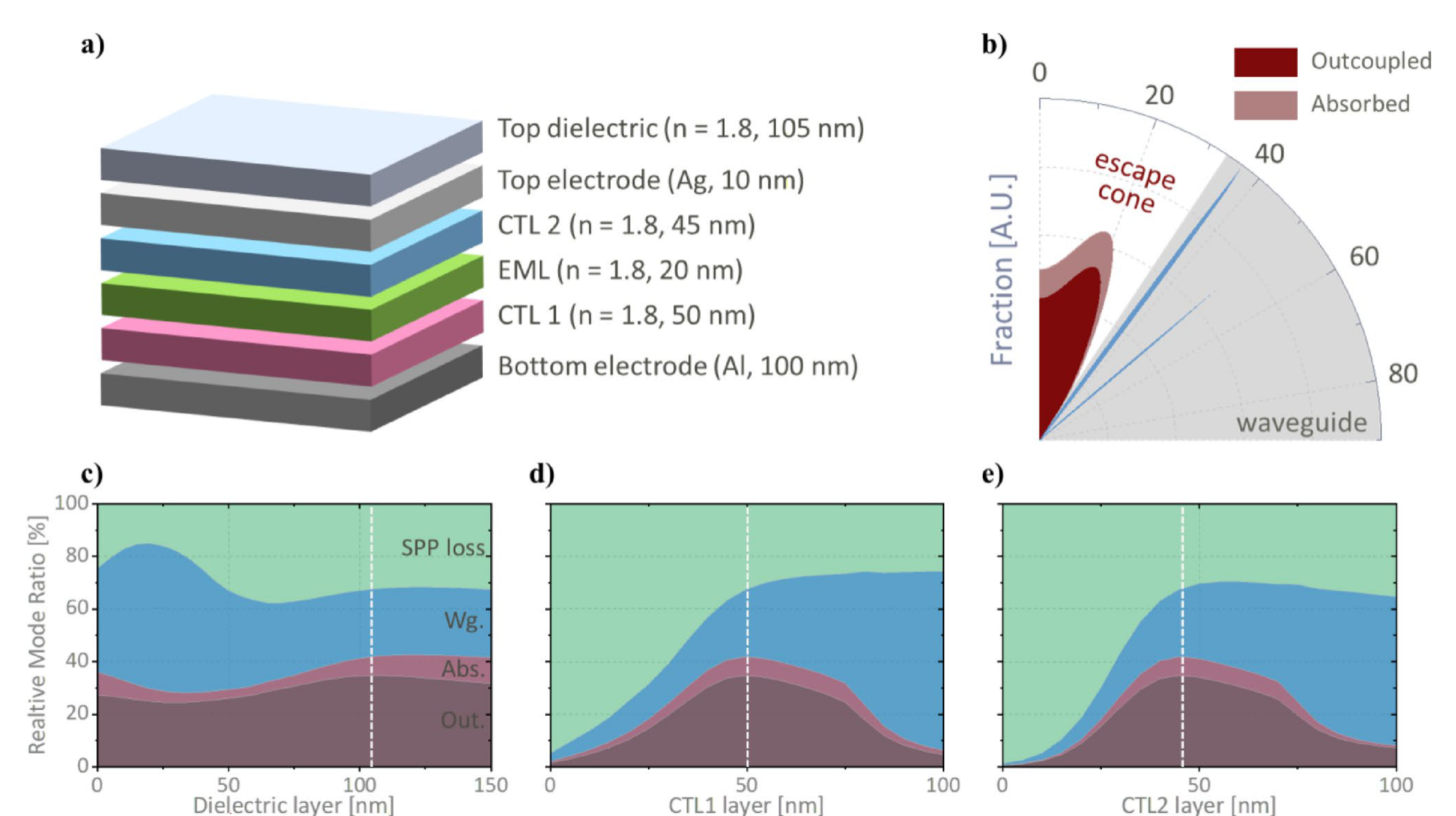
Journal: Macromolecular Research (2026) · Comparison target: Figure 1
The semitransparent Ag electrode and the Al reflector of a top-emitting OLED form a strong microcavity. For a laterally uniform planar device, a one-dimensional model is generally more accurate than FDTD. The paper's three-dimensional FDTD results show that the one-dimensional design remains valid above a pixel width of 1 μm, while edge effects must be considered at 1 μm or below. This case reproduces the internal angular power distribution, three thickness sweeps, and optical-power channel distribution of the laterally infinite device at 530 nm.
The published light-extraction efficiency of the optimum stack is 34.6%. With the same inputs, Dreapex TMM gives 34.32% top outcoupling, 25.83% waveguide power, 32.42% evanescent power, and 7.43% absorption. The largest absolute difference across the four channels is 0.28 percentage points.
Background
The one-dimensional model treats every layer as a laterally infinite plane. It therefore isolates how film thickness, propagation phase, and interface reflection set the microcavity resonance. Paper Figure 1c–e sweep Top dielectric, CTL1, and CTL2 in turn. The reflection phases of the two metal electrodes and the optical thicknesses of these three adjustable layers set the fraction of 530 nm emission that reaches the escape cone in air.
The paper divides total optical power into Outcoupled, Absorbed, Waveguide, and SPP loss. The software outputs are mapped as follows:
| Paper channel | Dreapex TMM channel | Meaning in this case |
|---|---|---|
| Outcoupled / LEE | Top Outcoupling | Power transmitted through the top dielectric into air |
| Absorbed | Absorption | Parasitic absorption in the Ag and Al electrodes |
| Wg. | Waveguide | Propagating power trapped in the planar stack beyond the air escape cone |
| SPP loss | Evanescent | High-in-plane-wavevector near-field channel, dominated here by coupling to metal surface plasmons |
This mapping gives channel-by-channel agreement at the optimum stack. The paper does not publish the numerical boundary of its SPP integral, so the remaining difference between Evanescent and SPP must still be read as a definition difference between the two models.
Structure
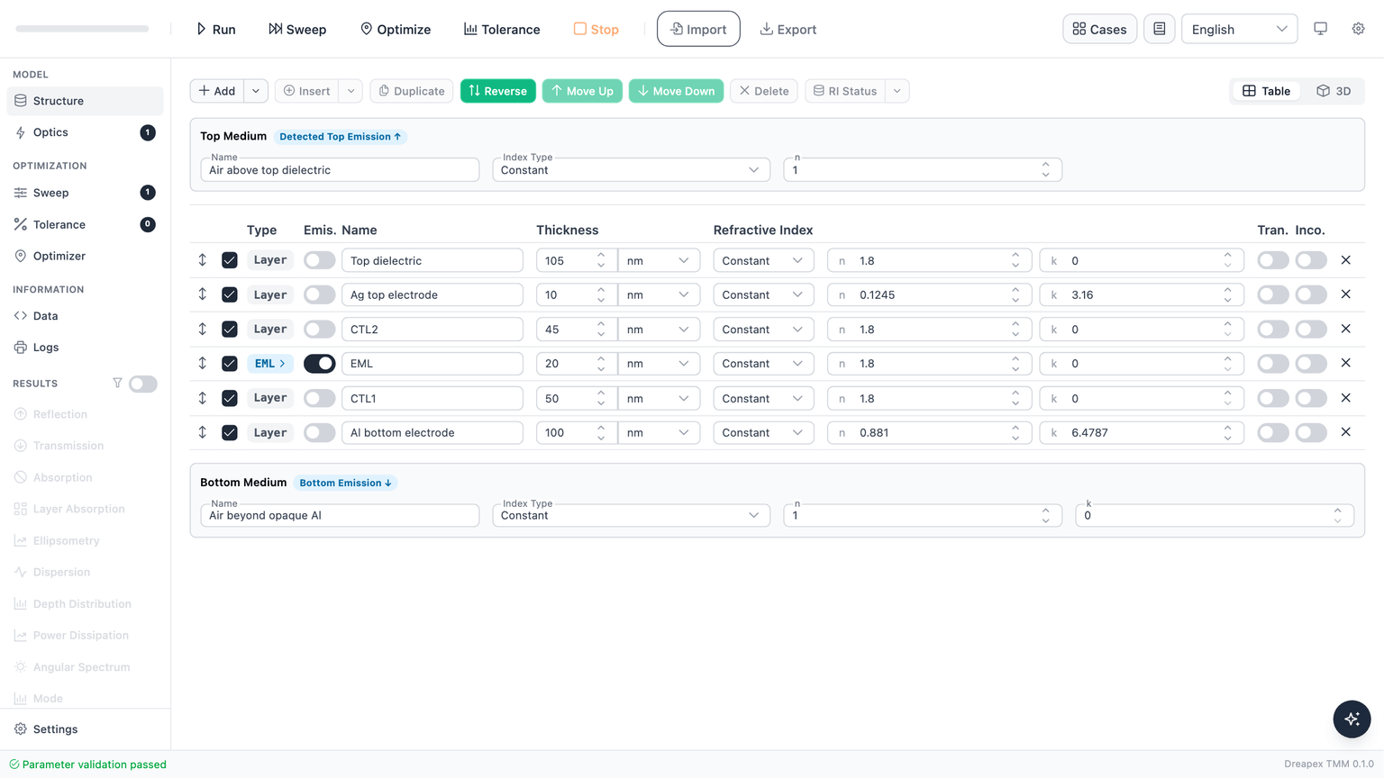
Build six finite layers from the top emission side toward the Al bottom electrode. The paper gives every optical constant directly at 530 nm, so the primary reproduction uses no material database and requires no continuous dispersion curve.
| Position | Material | Thickness | Optical constant at 530 nm |
|---|---|---|---|
Top Medium | Air | Semi-infinite | , |
| Layer 1 | Top dielectric | 105 nm | , |
| Layer 2 | Ag top electrode | 10 nm | , |
| Layer 3 | CTL2 | 45 nm | , |
| Layer 4 | EML | 20 nm | , |
| Layer 5 | CTL1 | 50 nm | , |
| Layer 6 | Al bottom electrode | 100 nm | , |
Bottom Medium | Air | Semi-infinite | , |
The medium behind the 100 nm Al film is not stated in the paper. This case sets the Bottom Medium to air. Bottom Outcoupling is only in the optimum stack, showing that the Al film effectively isolates the emitting cavity from that external boundary.
Emission and Sweep Settings
Place one 530 nm isotropic emitter at the middle of the EML. Isotropic is equivalent to the paper's separate x-, y-, and z-dipole calculations with one-third weight each. Set the relative position to 0.5, the spatial distribution to Delta, and Quantum Efficiency to 1. The last value closes the paper's optical-power budget at 100%; it does not claim that the physical emitter has a photoluminescence quantum yield of 100%.

Under Emission in Optics, enable only Mode, use Single wavelength mode, and enter 530 nm.

For Figure 1b, also enable Power Dissipation, select Effective Index (nEff), and use 0–1.8 with a 0.001 step. nEff = 1 is the air light line and nEff = 1.8 is the EML light line. The paper omits the SPP region, where the propagation angle is complex, so higher in-plane wavevectors are not sampled here.

Run the three sweeps separately rather than combining the thicknesses into a three-dimensional parameter grid. Keep every other thickness at its published optimum and vary only the listed parameter:
| Sweep | From | To | Step | Paper optimum |
|---|---|---|---|---|
structure / Top dielectric / thickness | 0 nm | 150 nm | 1 nm | 105 nm |
structure / CTL1 / thickness | 0 nm | 100 nm | 1 nm | 50 nm |
structure / CTL2 / thickness | 0 nm | 100 nm | 1 nm | 45 nm |
The Top dielectric sweep row is shown below. CTL1 and CTL2 use the same Step sampling with only the path and endpoint changed.

Simulation Results and Comparison with Figure 1
Internal angular power density (Figure 1b)
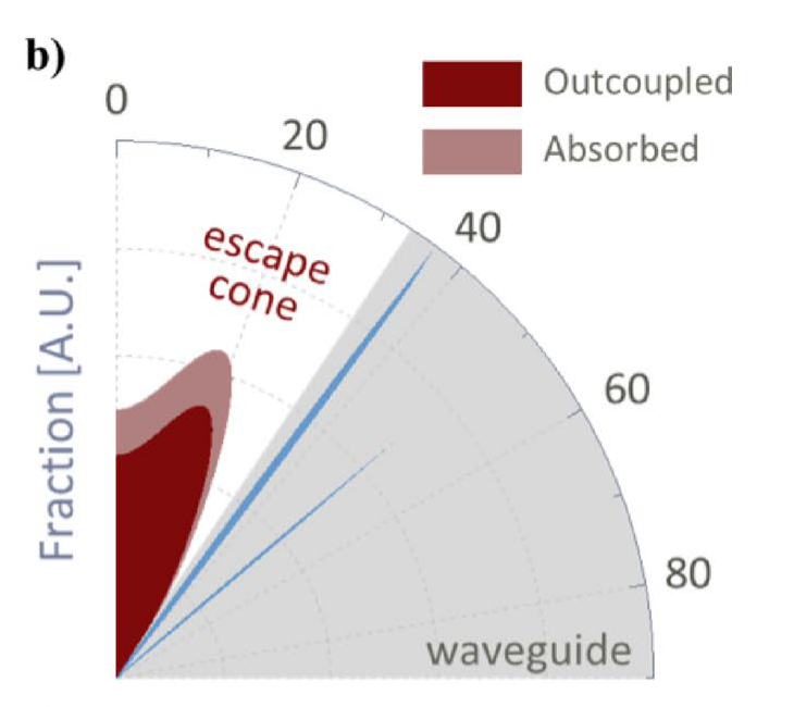
Paper Figure 1b uses the propagation angle inside the EML to show Outcoupled, Absorbed, and Waveguide power in the optimum structure, with angles above 33.7° marked as the waveguide region. Its radial axis uses arbitrary units, so this case compares only the critical angle, peak positions, and normalized curve shape, not absolute amplitude.
The next plot transforms the same 1,801-point result. Its filled bands and two blue waveguide peaks share one arbitrary-unit scale factor.
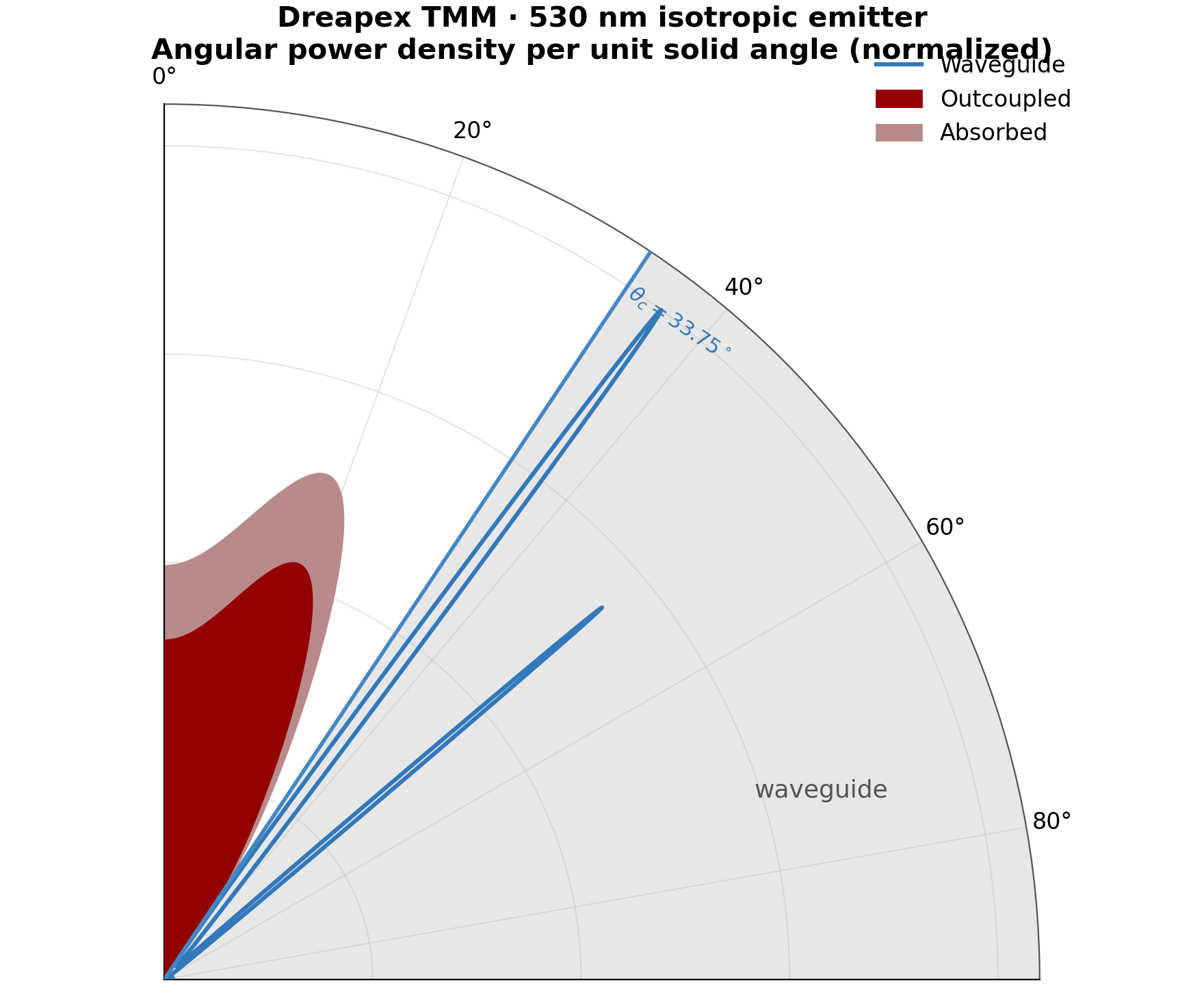
The published bands remain nonzero along the normal and reach their largest radius near 20°. The Dreapex TMM total-power and top-outcoupled profiles peak at 17.69° and 17.72°; their normal-direction values are 0.780 and 0.777 of their respective maxima. The critical angle calculated as is 33.75°, agreeing with the paper's 33.7°. The strongest calculated waveguide peak is at 36.59°, against 37.6° in the paper text, a difference of −1.01°. A second calculated peak at 49.66° agrees with the position of the second narrow peak in the published plot.
The native software page below preserves the source calculation. The Total / Total curve is ; the polar plot uses the real-angle range and applies the coordinate transformation above.
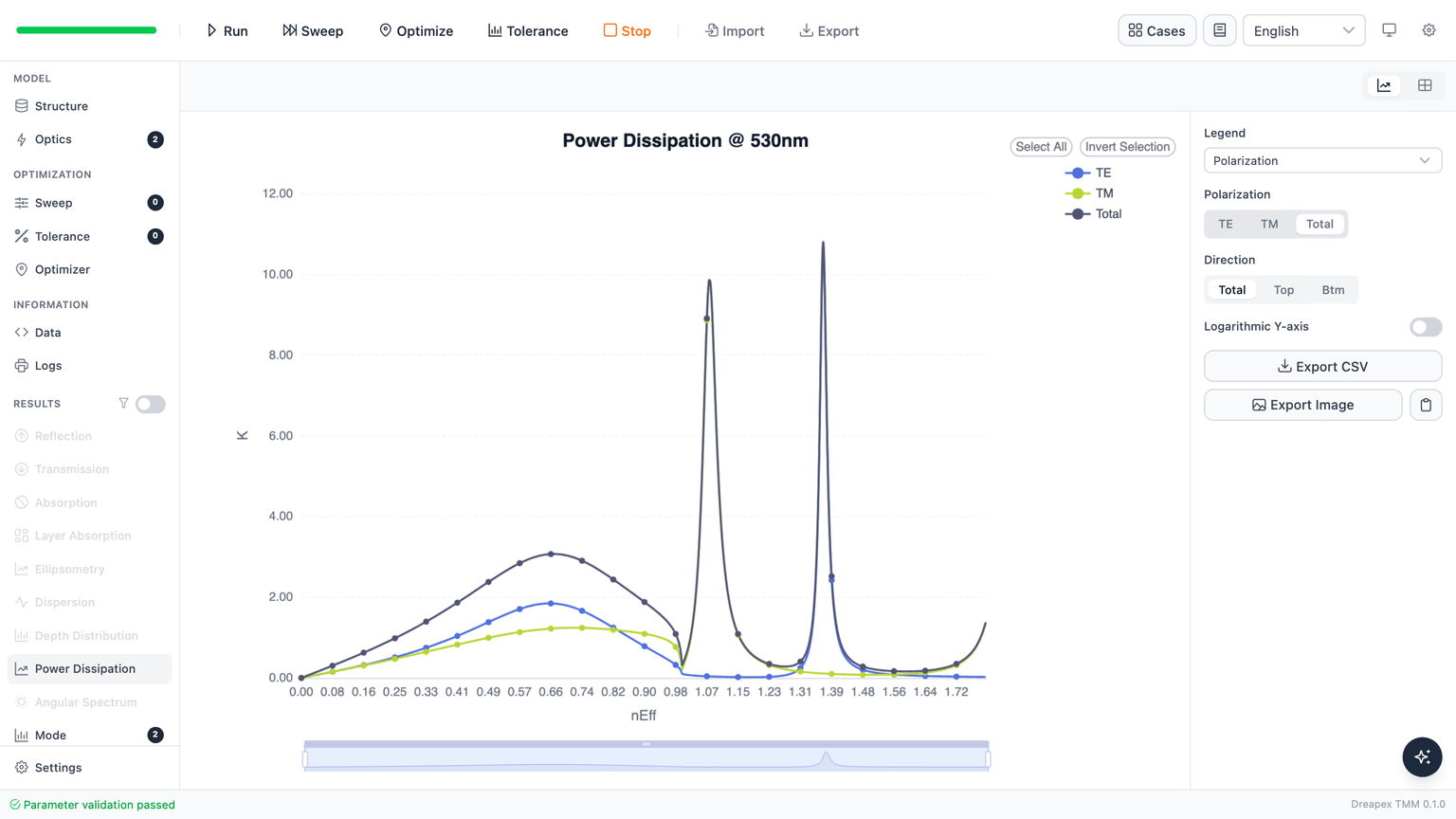
Integrating and normalizing by the Purcell factor from the same run reconstructs top outcoupling, absorption, and waveguide fractions of 34.32%, 7.43%, and 25.83%. Each agrees with the corresponding Mode channel within 0.01 percentage points, confirming that the polar plot and the channel fractions below use the same power budget.
Converting the CSV to internal angular power density
The exported from Power Dissipation is the azimuth-integrated in-plane-wavevector density of channel . Only the following two relations are needed in the real-propagation region to convert the horizontal coordinate to the internal EML angle and the radial value to power density per unit solid angle:
Here, , and denotes Outcoupled, Absorbed, or Waveguide. At , the smallest positive sample approximates the one-sided limit. Outcoupled and Absorbed use , while Waveguide uses ; all three channels share the maximum of the total spectrum over the real-propagation region.
Download the Dreapex TMM Power Dissipation CSV and place it beside the Python script below.
Install the dependencies before the first run:
python -m pip install pandas numpy matplotlib
Save the code as plot-angular-power-density.py, then run:
python plot-angular-power-density.py
The script reads the exported nEff, wavelength_nm, K_total, K_top_total, and K_btm_total columns, then writes angular-power-density.csv and angular-power-density.png.
from pathlib import Path

import matplotlib.pyplot as plt
import numpy as np
import pandas as pd

csv_path = Path("leda-power-dissipation.csv")
n_eml = 1.8

data = pd.read_csv(csv_path, encoding="utf-8-sig")
data = (
    data.loc[
        np.isclose(data["wavelength_nm"], 530.0)
        & data["nEff"].between(0.0, n_eml)
    ]
    .sort_values("nEff")
    .reset_index(drop=True)
)

n_eff = data["nEff"].to_numpy(dtype=float)
theta = np.arcsin(n_eff / n_eml)
jacobian = np.full_like(n_eff, np.nan)
positive = n_eff > 0
jacobian[positive] = (
    n_eml**2 * np.cos(theta[positive])
    / (2 * np.pi * n_eff[positive])
)

k_total = data["K_total"].to_numpy(dtype=float)
k_top = data["K_top_total"].to_numpy(dtype=float)
k_bottom = data["K_btm_total"].to_numpy(dtype=float)
k_absorbed = np.maximum(0.0, k_total - k_top - k_bottom)
escape = n_eff <= 1.0

data["theta_deg"] = np.degrees(theta)
data["total"] = k_total * jacobian
data["outcoupled"] = np.where(escape, k_top * jacobian, 0.0)
data["absorbed"] = np.where(escape, k_absorbed * jacobian, 0.0)
data["waveguide"] = np.where(~escape, k_total * jacobian, 0.0)

# nEff = 0 gives 0/0; use the smallest positive sample as the right-hand limit.
first_positive = np.flatnonzero(positive)[0]
zero = ~positive
channels = ["total", "outcoupled", "absorbed", "waveguide"]
data.loc[zero, channels] = data.loc[first_positive, channels].to_numpy()

# Every channel uses the same normalization factor.
scale = data["total"].max()
data[channels] = data[channels] / scale
data.to_csv("angular-power-density.csv", index=False)

theta = np.radians(data["theta_deg"].to_numpy())
waveguide = ~escape
fig, ax = plt.subplots(figsize=(7, 6), subplot_kw={"projection": "polar"})
ax.fill_between(
    theta[escape],
    0,
    (data.loc[escape, "outcoupled"] + data.loc[escape, "absorbed"]),
    color="#b98a8a",
    label="Absorbed",
)
ax.fill_between(
    theta[escape], 0, data.loc[escape, "outcoupled"],
    color="#940000", label="Outcoupled",
)
ax.plot(
    theta[waveguide], data.loc[waveguide, "waveguide"],
    color="#3279bb", label="Waveguide",
)
ax.set_theta_zero_location("N")
ax.set_theta_direction(-1)
ax.set_thetamin(0)
ax.set_thetamax(90)
ax.legend()
fig.tight_layout()
fig.savefig("angular-power-density.png", dpi=200, facecolor="white")
Three thickness sweeps (Figure 1c–e)
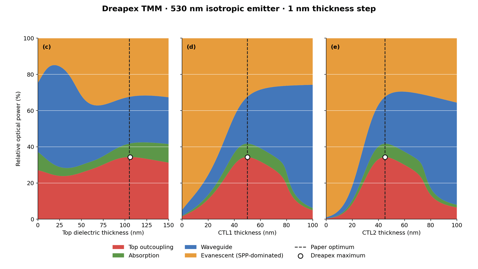
The four filled bands in paper Figure 1c–e give the relative optical powers from the three single-parameter sweeps. White dashed lines mark the published optimum thicknesses.
The next graphic was independently drawn from 353 real Mode calculations, with the channel order matched to the paper. Dashed lines are the published optimum thicknesses; black points are the Dreapex TMM maxima in top outcoupling.
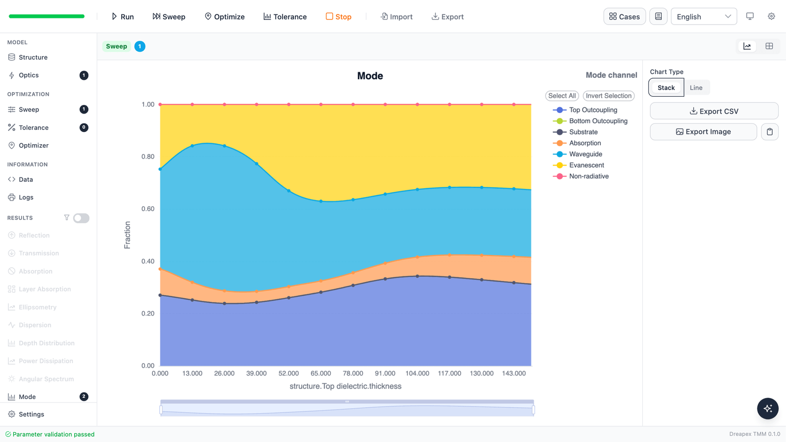
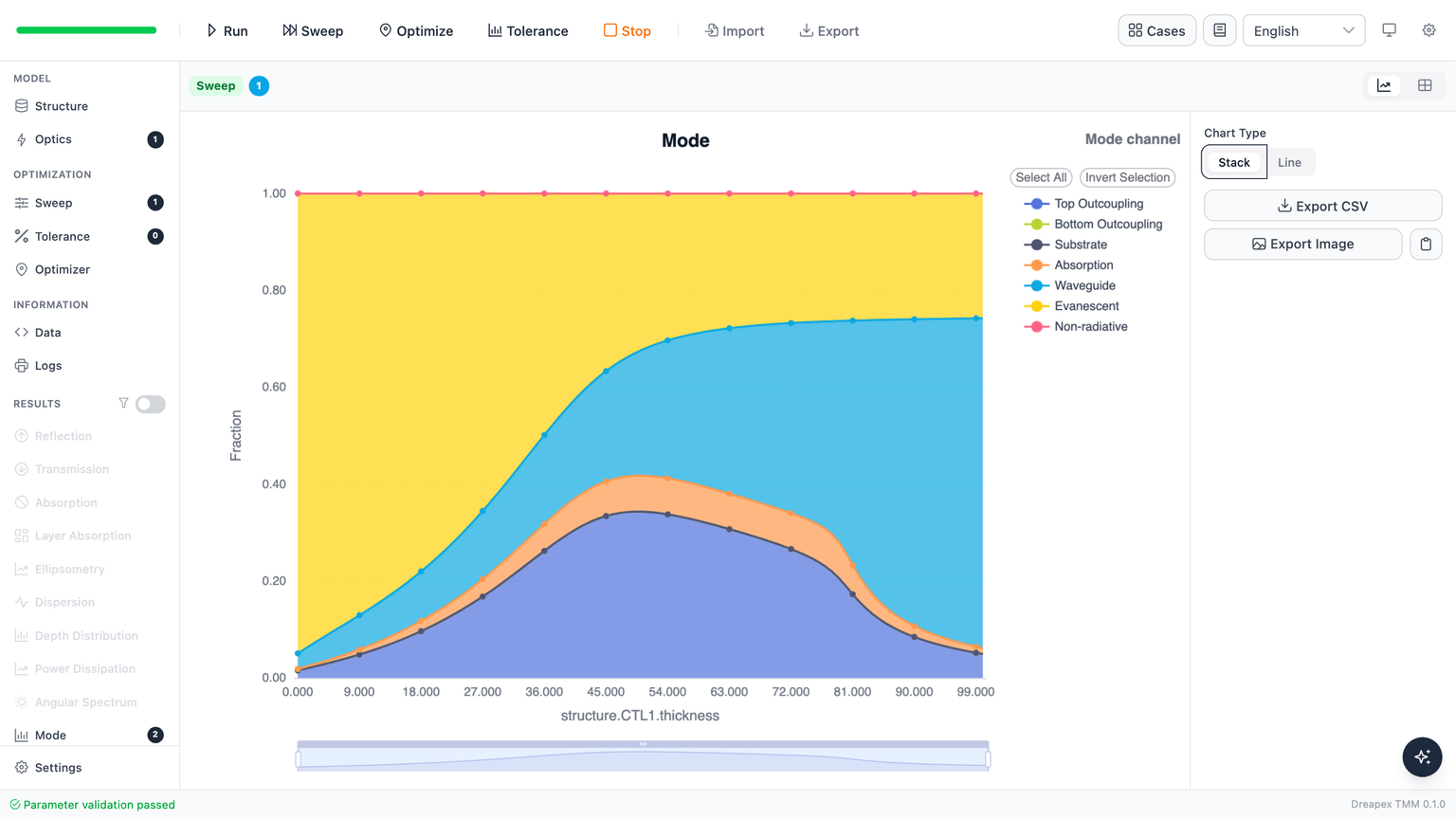
The following three software result pages preserve the native interface evidence for each sweep. Each page shows one Sweep at the upper left, the actual parameter path on the horizontal axis, Stack selected under Chart Type, and successful parameter validation in the footer.
The Top dielectric result holds CTL1 at 50 nm and CTL2 at 45 nm while covering 0–150 nm. Top outcoupling reaches its maximum at 106 nm, against the paper's dashed line at 105 nm.
The CTL1 result holds Top dielectric at 105 nm and CTL2 at 45 nm while covering 0–100 nm. Its top-outcoupling maximum occurs at the published 50 nm.
The CTL2 result holds Top dielectric at 105 nm and CTL1 at 50 nm while covering 0–100 nm. Its top-outcoupling maximum occurs at the published 45 nm.
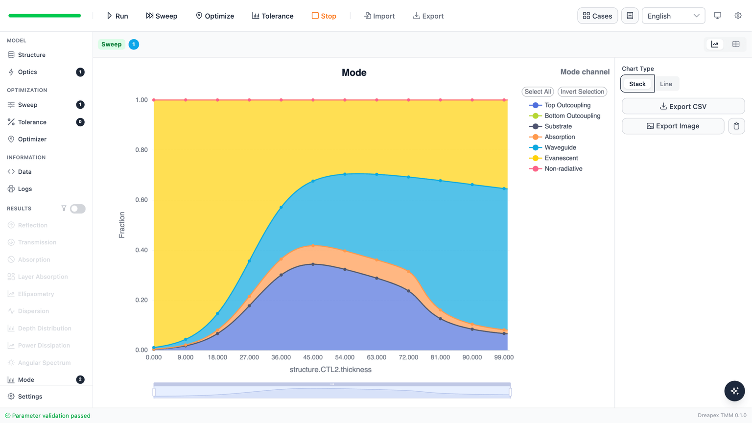
The peaks in all three top-outcoupling curves agree with the paper to within one sweep step:
| Sweep | Paper optimum | Dreapex TMM optimum | Thickness difference | Peak top outcoupling |
|---|---|---|---|---|
| Top dielectric | 105 nm | 106 nm | +1 nm | 34.33% |
| CTL1 | 50 nm | 50 nm | 0 nm | 34.32% |
| CTL2 | 45 nm | 45 nm | 0 nm | 34.32% |
The minimum top outcoupling in the Top dielectric sweep is 23.82%, against the published lower bound of 24.3%. At zero thickness, CTL1 gives 1.54% and CTL2 gives 0.36%, consistent with the paper's stated range of about 1% to 34.6% and its rapid fall near zero thickness.
One Mode run at the published optimum thicknesses of 105 / 50 / 45 nm gives the following raw software result:
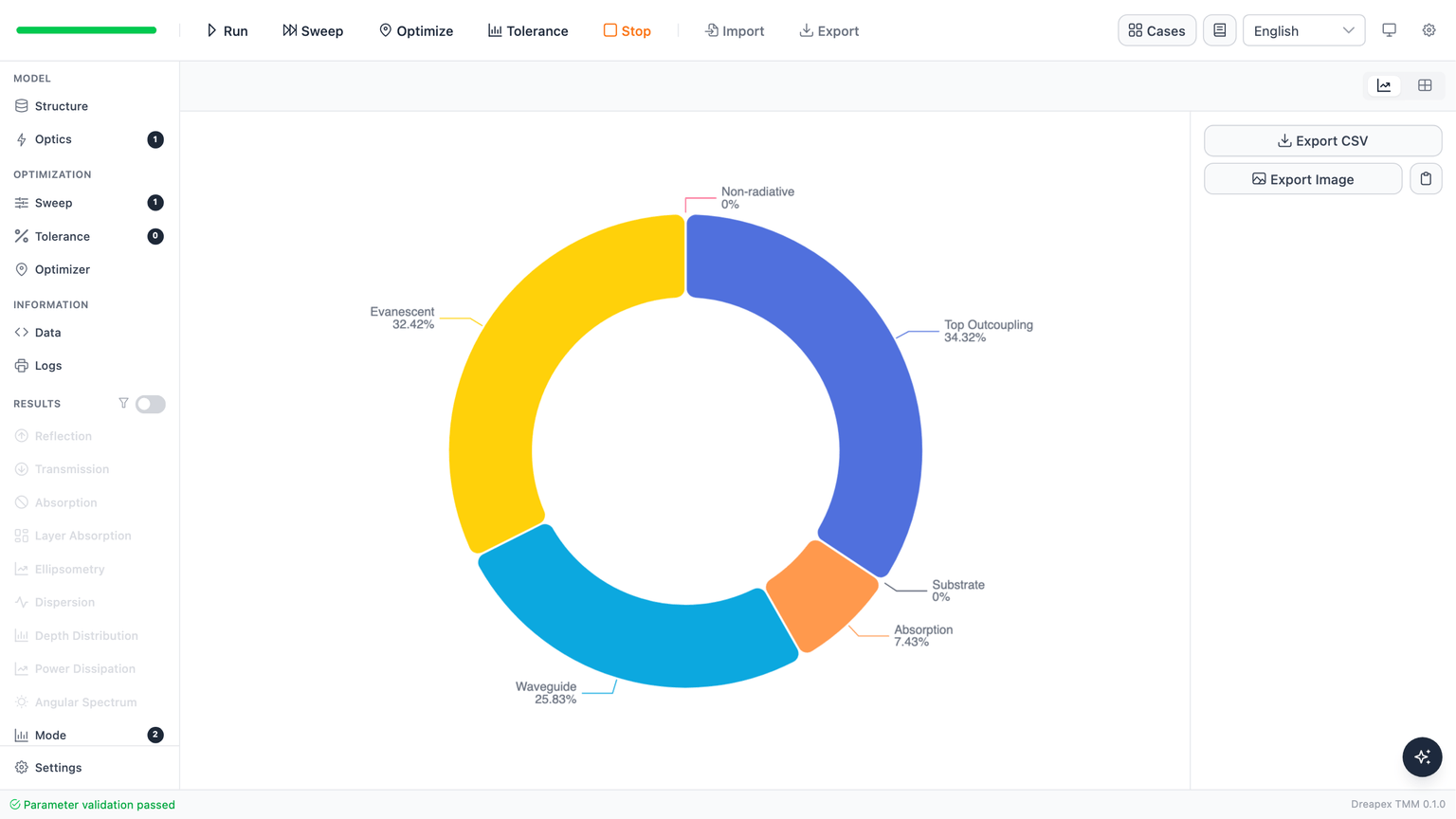
| Optical-power channel | Paper | Dreapex TMM | Difference |
|---|---|---|---|
| Top outcoupling | 34.6% | 34.32% | −0.28 pp |
| Waveguide | 25.7% | 25.83% | +0.13 pp |
| SPP / Evanescent | 32.5% | 32.42% | −0.08 pp |
| Absorption | 7.2% | 7.43% | +0.23 pp |
| Total | 100.0% | 100.00% | 0.00 pp |
Deviation Notes
- Figure 1c–e has no numerical source data, so the comparison covers peak and valley positions, direction of change, and magnitude rather than point-by-point RMS.
- Figure 1b uses arbitrary radial units, so only the critical angle, peak positions, and normalized curve shape are compared.
- The paper does not give the full integration boundaries for SPP, waveguide, and absorption; the maximum difference across the four channels at the optimum stack is
0.28 pp.